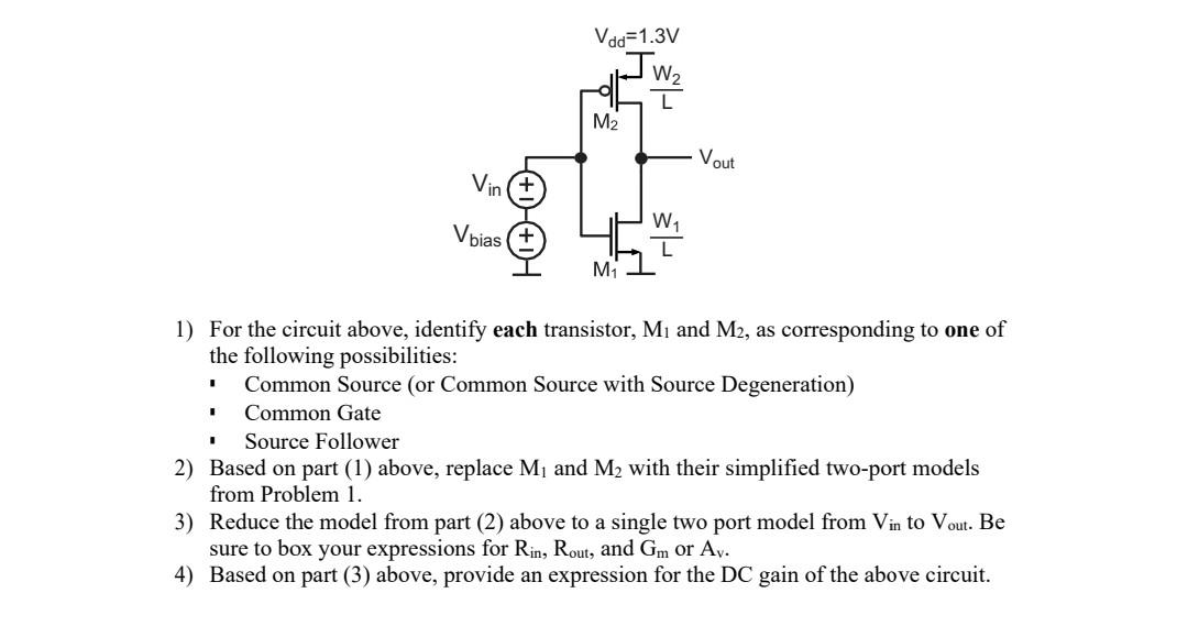
1) For the circuit above, identify each transistor, M1 and M2, as corresponding to one of the following possibilities: Common Source (or Common Source with Source Degeneration) Common Gate Source Follower 2) Based on part (1) above, replace M1 and M2 with their simplified two-port models from Problem 1. 3) Reduce the model from part (2) above to a single two port model from Vin to Vout. Be sure to box your expressions for Rin, Rout, and Gm or Av. 4) Based on part (3) above, provide an expression for the DC gain of the above circuit.


You'll get a detailed, step-by-step and expert verified solution.
 Work With Experts to Reach at Correct Answers