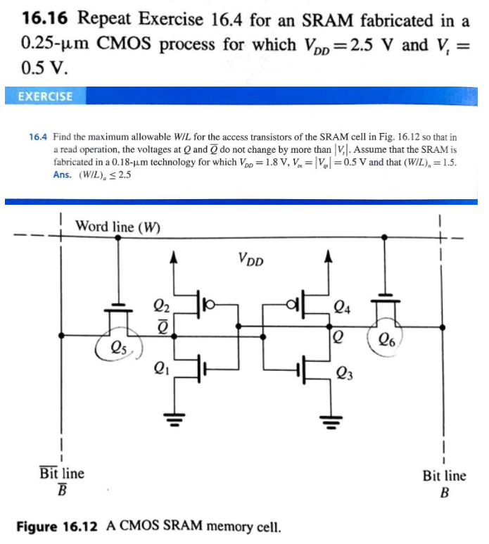
16.16 Repeat Exercise 16.4 for an SRAM fabricated in a 0.25−μm CMOS process for which VDD = 2.5 V and Vt = 0.5 V. EXERCISE 16.4 Find the maximum allowable W/L for the access transistors of the SRAM cell in Fig. 16.12 so that in a read operation, the voltages at Q and Q¯ do not change by more than |Vt|. Assume that the SRAM is fabricated in a 0.18−μm technology for which VDD = 1.8 V, Vtx = |Vφ| = 0.5 V and that (W/L)n = 1.5. Ans. (W/L)a ≤ 2.5 Figure 16.12 A CMOS SRAM memory cell.
16.16 Repeat Exercise 16.4 for an SRAM fabricated in a 0.25−μm CMOS process for which VDD = 2.5 V and Vt = 0.5 V. EXERCISE 16.4 Find the maximum allowable W/L for the access transistors of the SRAM cell in Fig. 16.12 so that in a read operation, the voltages at Q and Q¯ do not change by more than |Vt|. Assume that the SRAM is fabricated in a 0.18−μm technology for which VDD = 1.8 V, Vtx = |Vφ| = 0.5 V and that (W/L)n = 1.5. Ans. (W/L)a ≤ 2.5 Figure 16.12 A CMOS SRAM memory cell.

Image text
16.16 Repeat Exercise 16.4 for an SRAM fabricated in a 0.25 μ m CMOS process for which V D D = 2.5 V and V t = 0.5 V . EXERCISE 16.4 Find the maximum allowable W/L for the access transistors of the SRAM cell in Fig. 16.12 so that in a read operation, the voltages at Q and Q ¯ do not change by more than | V t | . Assume that the SRAM is fabricated in a 0.18 μ m technology for which V D D = 1.8 V , V t x = | V φ | = 0.5 V and that ( W / L ) n = 1.5 . Ans. ( W / L ) a 2.5
Figure 16.12 A CMOS SRAM memory cell.

Detailed Answer