2-Consider the Circuit below a-)What is the logic function implemented by the CMOS transistor network? b-)Size the NMOS and PMOS devices so that the output resistance is the same as that of an inverter with an NMOS W/L = 4 and PMOS W/L = 8. C-) If P(A = 1) = 0.5, P(B = 1) = 0.2, P(C = 1) = 0.3 and P(D = 1) = 1, determine the power dissipation in the logic gate. Assume VDD=2.5V, Cout = 30 fF and fclk = 250 MHz. (To find the switching activity you must calculate the Pγ(0−1) = Pγ=1×Pγ=0 = Pγ=0×(1−Pγ=1)
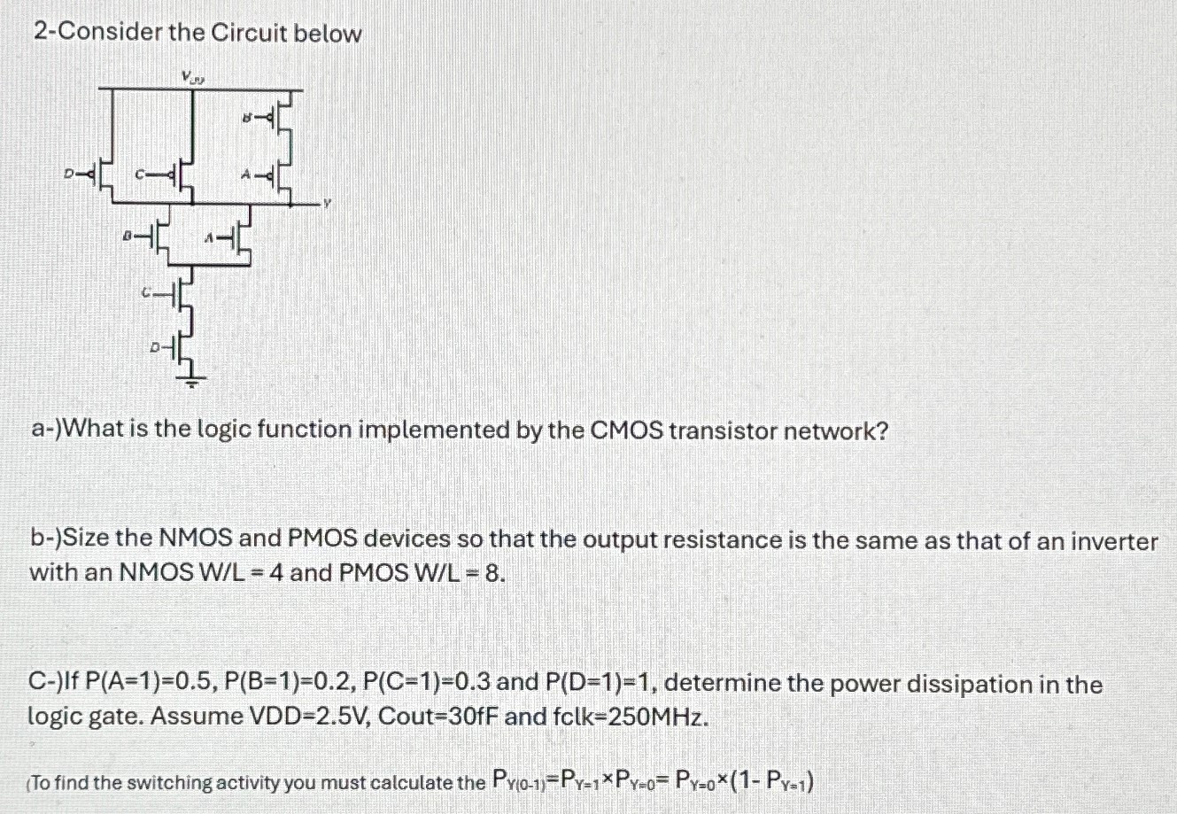
2-Consider the Circuit below a-)What is the logic function implemented by the CMOS transistor network? b-)Size the NMOS and PMOS devices so that the output resistance is the same as that of an inverter with an NMOS W/L = 4 and PMOS W/L = 8. C-) If P(A = 1) = 0.5, P(B = 1) = 0.2, P(C = 1) = 0.3 and P(D = 1) = 1, determine the power dissipation in the logic gate. Assume VDD=2.5V, Cout = 30 fF and fclk = 250 MHz. (To find the switching activity you must calculate the Pγ(0−1) = Pγ=1×Pγ=0 = Pγ=0×(1−Pγ=1)

Image text
2-Consider the Circuit below a-)What is the logic function implemented by the CMOS transistor network? b-)Size the NMOS and PMOS devices so that the output resistance is the same as that of an inverter with an N M O S W / L = 4 and P M O S W / L = 8 .
C-) If P ( A = 1 ) = 0.5 , P ( B = 1 ) = 0.2 , P ( C = 1 ) = 0.3 and P ( D = 1 ) = 1 , determine the power dissipation in the logic gate. Assume VDD=2.5V, Cout = 30 f F and fclk = 250 M H z . (To find the switching activity you must calculate the P Y ( 0 1 ) = P Y = 1 × P Y = 0 = P Y = 0 × ( 1 P Y = 1 )

Detailed Answer