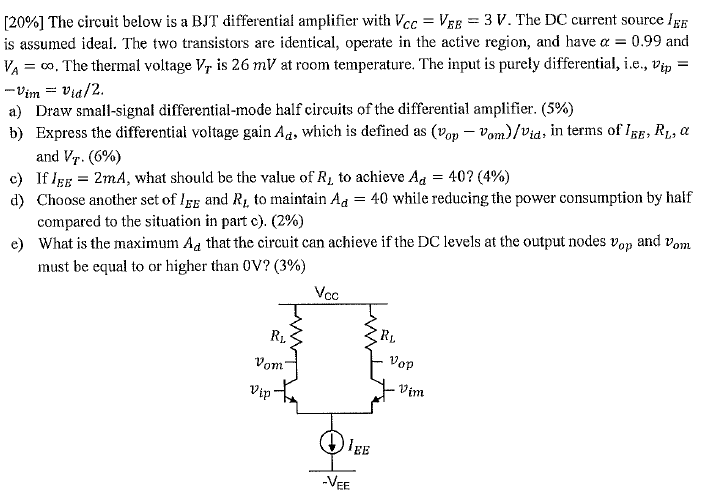
[20%] The circuit below is a BJT differential amplifier with VCC = VEE = 3 V. The DC current source IEE is assumed ideal. The two transistors are identical, operate in the active region, and have α = 0.99 and VA = ∞. The thermal voltage VT is 26 mV at room temperature. The input is purely differential, i. e. , vip = −vim = vid/2 a) Draw small-signal differential-mode half circuits of the differential amplifier. ( 5%) b) Express the differential voltage gain Ad, which is defined as (vop−vom)/vid, in terms of IEE, RL, α and VT⋅(6%) c) If IEE = 2 mA, what should be the value of RL to achieve Ad = 40 ? (4%) d) Choose another set of IEE and RL to maintain Ad = 40 while reducing the power consumption by half compared to the situation in part c). (2%) e) What is the maximum Ad that the circuit can achieve if the DC levels at the output nodes vop and vom must be equal to or higher than 0 V? (3%)
![[20%] The circuit below is a BJT differential amplifier with VCC = VEE = 3 V. The DC current source IEE is assumed ideal. The two transistors are identical, operate in the active region, and have α = 0.99 and VA = ∞. The thermal voltage VT is 26 mV at room temperature. The input is purely differential, i. e. , vip = −vim = vid/2 a) Draw small-signal differential-mode half circuits of the differential amplifier. ( 5%) b) Express the differential voltage gain Ad, which is defined as (vop−vom)/vid, in terms of IEE, RL, α and VT⋅(6%) c) If IEE = 2 mA, what should be the value of RL to achieve Ad = 40 ? (4%) d) Choose another set of IEE and RL to maintain Ad = 40 while reducing the power consumption by half compared to the situation in part c). (2%) e) What is the maximum Ad that the circuit can achieve if the DC levels at the output nodes vop and vom must be equal to or higher than 0 V? (3%)](https://www.doubtrix.com/uploads/editor/8985993089jYTQXcfJDH.png)