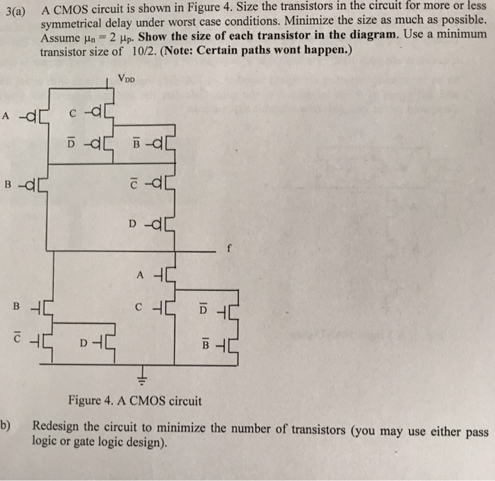
3(a) A CMOS circuit is shown in Figure 4. Size the transistors in the circuit for more or less symmetrical delay under worst case conditions. Minimize the size as much as possible. Assume un = 2up. Show the size of each transistor in the diagram. Use a minimum transistor size of 10/2. (Note: Certain paths wont happen.) b) Redesign the circuit to minimize the number of transistors (you may use either pass logic or gate logic design).