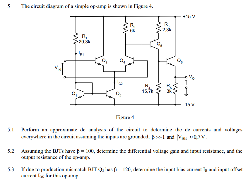
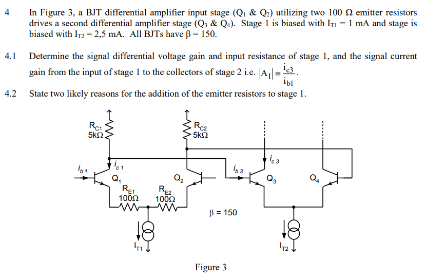
4 In Figure 3, a BJT differential amplifier input stage (Q1 & Q2) utilizing two 100 Ω emitter resistors drives a second differential amplifier stage (Q3&Q4). Stage 1 is biased with IT1 = 1 mA and stage is biased with IT2 = 2,5 mA. All BJTs have β = 150.4.1 Determine the signal differential voltage gain and input resistance of stage 1 , and the signal current gain from the input of stage 1 to the collectors of stage 2 i. e. |AI|≡ic3 ib1. 4.2 State two likely reasons for the addition of the emitter resistors to stage 1. Figure 3

![Consider a BJT differential amplifier biased with a Widlar current source, as shown in Figure 4. The transistor parameters are: β = 200, VBE(ON) = 0.7 V (except for Q3 and Q4), VA = ∞ for Q1 and Q2, and VA = 100 V for Q3 and Q4. Reverse saturation current, Is for transistor Q3 and Q4 is given as 1×10⁻¹⁵ A. From analysis, it is determined that I1 = 0.5 mA, la = 400 μA, v1 = v2 = 0 V, VCE2 = 2.7 V and CMRR (dB) = 80 dB Figure 4 a) Calculate the value of resistors R1, R2 and RC. b) Find the amplifier's differential-mode voltage gain (Ad), common-mode voltage gain (ACM) and common-mode output resistance ( Ricm ). [Ricm ≈ (1+β)Rocs where Rocs is the output resistance of the current source ] c) Draw the pnp version for the differential amplifier of Figure 4. Clearly label all resistors and currents.](https://www.doubtrix.com/uploads/editor/6551442834FjRRsYNstK.jpg)