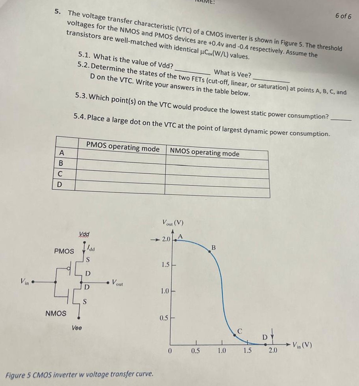
5. The voltage transfer characteristic (VTC) of a CMOS inverter is shown in Figure 5 . The threshold voltages for the NMOS and PMOS devices are +0.4V and -0.4 respectively. Assume the transistors are well-matched with identical μCox(W/L) values. 5.1. What is the value of Vdd? What is Vee? 5.2. Determine the states of the two FETs (cut-off, linear, or saturation) at points A, B, C, and D on the VTC. Write your answers in the table below. 5.3. Which point(s) on the VTC would produce the lowest static power consumption? 5.4. Place a large dot on the VTC at the point of largest dynamic power consumption.Figure 5 CMOS inverter w voltage transfer curve.
5. The voltage transfer characteristic (VTC) of a CMOS inverter is shown in Figure 5 . The threshold voltages for the NMOS and PMOS devices are +0.4V and -0.4 respectively. Assume the transistors are well-matched with identical μCox(W/L) values. 5.1. What is the value of Vdd? What is Vee? 5.2. Determine the states of the two FETs (cut-off, linear, or saturation) at points A, B, C, and D on the VTC. Write your answers in the table below. 5.3. Which point(s) on the VTC would produce the lowest static power consumption? 5.4. Place a large dot on the VTC at the point of largest dynamic power consumption.Figure 5 CMOS inverter w voltage transfer curve.

Image text
6 of 6 5. The voltage transfer characteristic (VTC) of a CMOS inverter is shown in Figure 5 . The threshold voltages for the NMOS and PMOS devices are + 0.4 V and -0.4 respectively. Assume the transistors are well-matched with identical μ C 0 o x ( W / L ) values. 5.1. What is the value of Vdd? What is Vee? 5.2. Determine the states of the two FETs (cut-off, linear, or saturation) at points A, B, C, and D on the VTC. Write your answers in the table below. 5.3. Which point(s) on the VTC would produce the lowest static power consumption? 5.4. Place a large dot on the VTC at the point of largest dynamic power consumption.
Figure 5 CMOS inverter w voltage transfer curve.

Detailed Answer