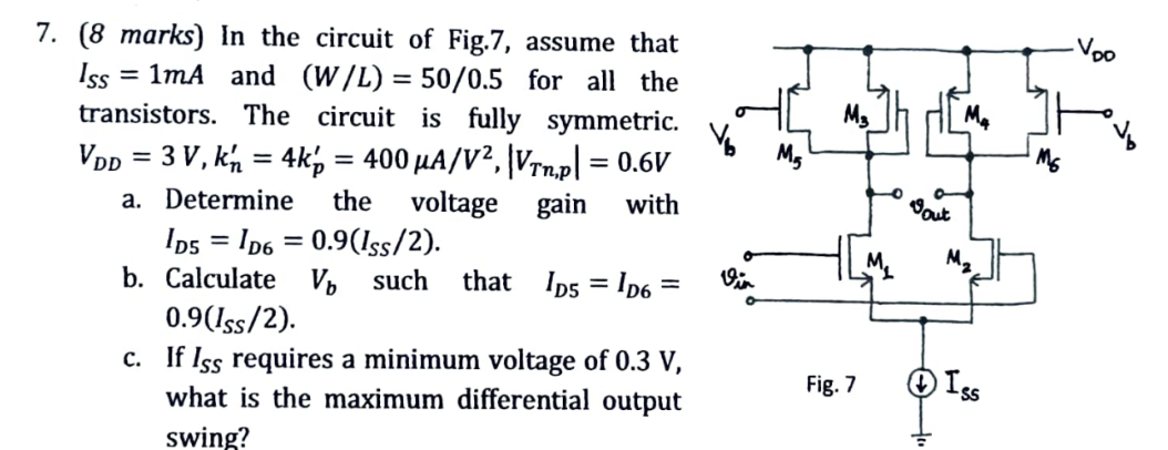
7 (8 marks) In the circuit of Fig. 7, assume that ISS = 1 mA and (W/L) = 50/0.5 for all the transistors. The circuit is fully symmetric. VDD = 3 V, kn′ = 4kp′ = 400 μA/V2, |VTn,p| = 0.6 V a. Determine the voltage gain with ID5 = ID6 = 0.9(ISS/2). b. Calculate Vb such that ID5 = ID6 = 0.9(ISS/2). c. If ISS requires a minimum voltage of 0. 3 V, what is the maximum differential output swing?