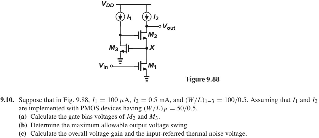
9.10. Suppose that in Fig. 9.88, I1 = 100 μA, I2 = 0.5 mA, and (W/L)1−3 = 100 /0.5. Assuming that I1 and I2 are implemented with PMOS devices having (W/L)P = 50 /0.5, (a) Calculate the gate bias voltages of M2 and M3. (b) Determine the maximum allowable output voltage swing. (c) Calculate the overall voltage gain and the input-referred thermal noise voltage.