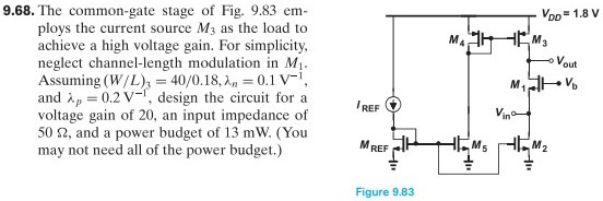
9.68. The common-gate stage of Fig. 9.83 employs the current source M3 as the load to achieve a high voltage gain. For simplicity, neglect channel-length modulation in M1. Assuming (W/L)3 = 40/0.18, λn = 0.1 V−1, and λp = 0.2 V−1, design the circuit for a voltage gain of 20, an input impedance of 50 Ω, and a power budget of 13 mW. (You may not need all of the power budget.) Figure 9.83
9.68. The common-gate stage of Fig. 9.83 employs the current source M3 as the load to achieve a high voltage gain. For simplicity, neglect channel-length modulation in M1. Assuming (W/L)3 = 40/0.18, λn = 0.1 V−1, and λp = 0.2 V−1, design the circuit for a voltage gain of 20, an input impedance of 50 Ω, and a power budget of 13 mW. (You may not need all of the power budget.) Figure 9.83

Image text
9.68. The common-gate stage of Fig. 9.83 employs the current source M 3 as the load to achieve a high voltage gain. For simplicity, neglect channel-length modulation in M 1 . Assuming ( W / L ) 3 = 40 / 0.18 , λ n = 0.1 V 1 , and λ p = 0.2 V 1 , design the circuit for a voltage gain of 20 , an input impedance of 50 Ω , and a power budget of 13 mW . (You may not need all of the power budget.)
Figure 9.83

Detailed Answer