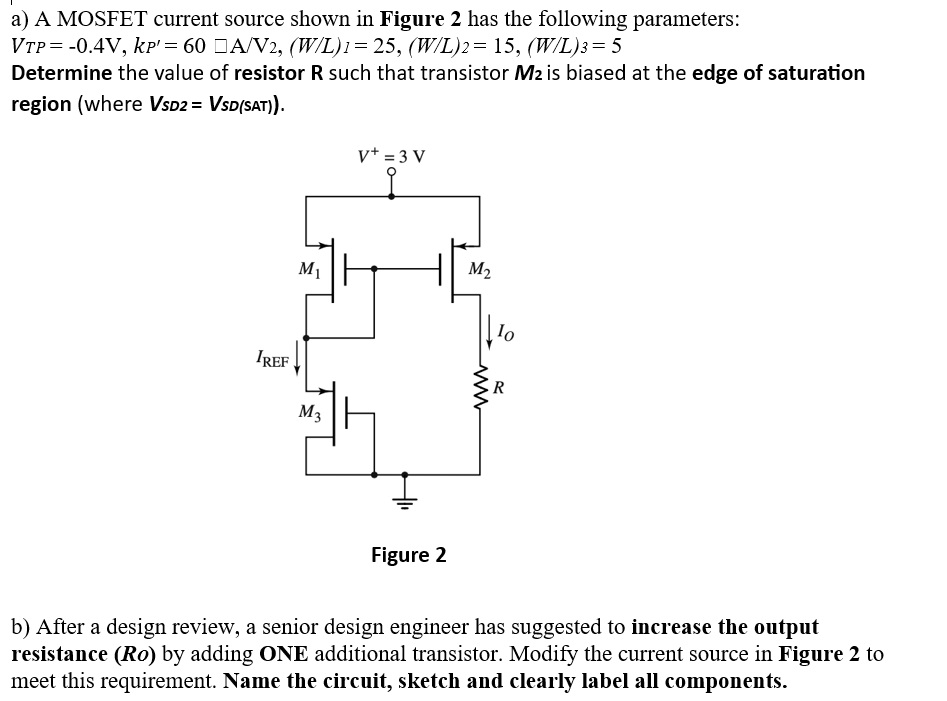
a) A MOSFET current source shown in Figure 2 has the following parameters: VTP = −0.4 V, kP′ = 60 μA/V2, (W/L)1 = 25, (W/L)2 = 15, (W/L)3 = 5 Determine the value of resistor R such that transistor M2 is biased at the edge of saturation region (where VSD2 = VSD(SAT)). Figure 2 b) After a design review, a senior design engineer has suggested to increase the output resistance (Ro) by adding ONE additional transistor. Modify the current source in Figure 2 to meet this requirement. Name the circuit, sketch and clearly label all components.
a) A MOSFET current source shown in Figure 2 has the following parameters: VTP = −0.4 V, kP′ = 60 μA/V2, (W/L)1 = 25, (W/L)2 = 15, (W/L)3 = 5 Determine the value of resistor R such that transistor M2 is biased at the edge of saturation region (where VSD2 = VSD(SAT)). Figure 2 b) After a design review, a senior design engineer has suggested to increase the output resistance (Ro) by adding ONE additional transistor. Modify the current source in Figure 2 to meet this requirement. Name the circuit, sketch and clearly label all components.

Image text
a) A MOSFET current source shown in Figure 2 has the following parameters:
V T P = 0.4 V , k P = 60 A / V 2 , ( W / L ) 1 = 25 , ( W / L ) 2 = 15 , ( W / L ) 3 = 5
Determine the value of resistor R such that transistor M 2 is biased at the edge of saturation region (where V S D 2 = V S D ( S A T ) ).
Figure 2
b) After a design review, a senior design engineer has suggested to increase the output resistance ( R o ) by adding ONE additional transistor. Modify the current source in Figure 2 to meet this requirement. Name the circuit, sketch and clearly label all components.

Detailed Answer