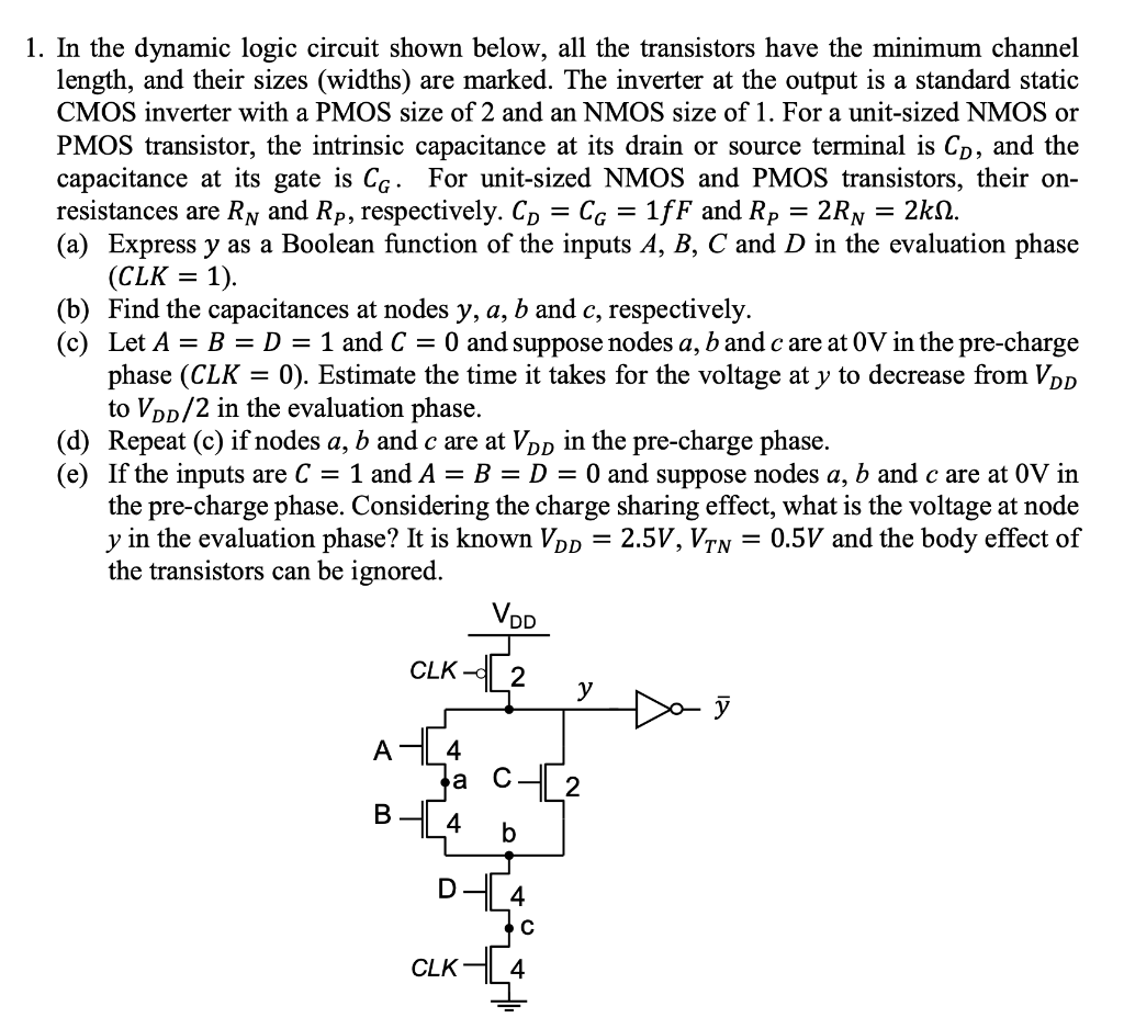
(A) Design a CMOS inverter in LTSpice environment with VDD = 1.8 V. (B) Consider the pull-down network (PDN) given as follows:Calculate the logic function of the given circuit topology. Implement the pull-up network (PUN) of the function. Size the transistors so the gate will operate similar to an optimized inverter with β = 2.