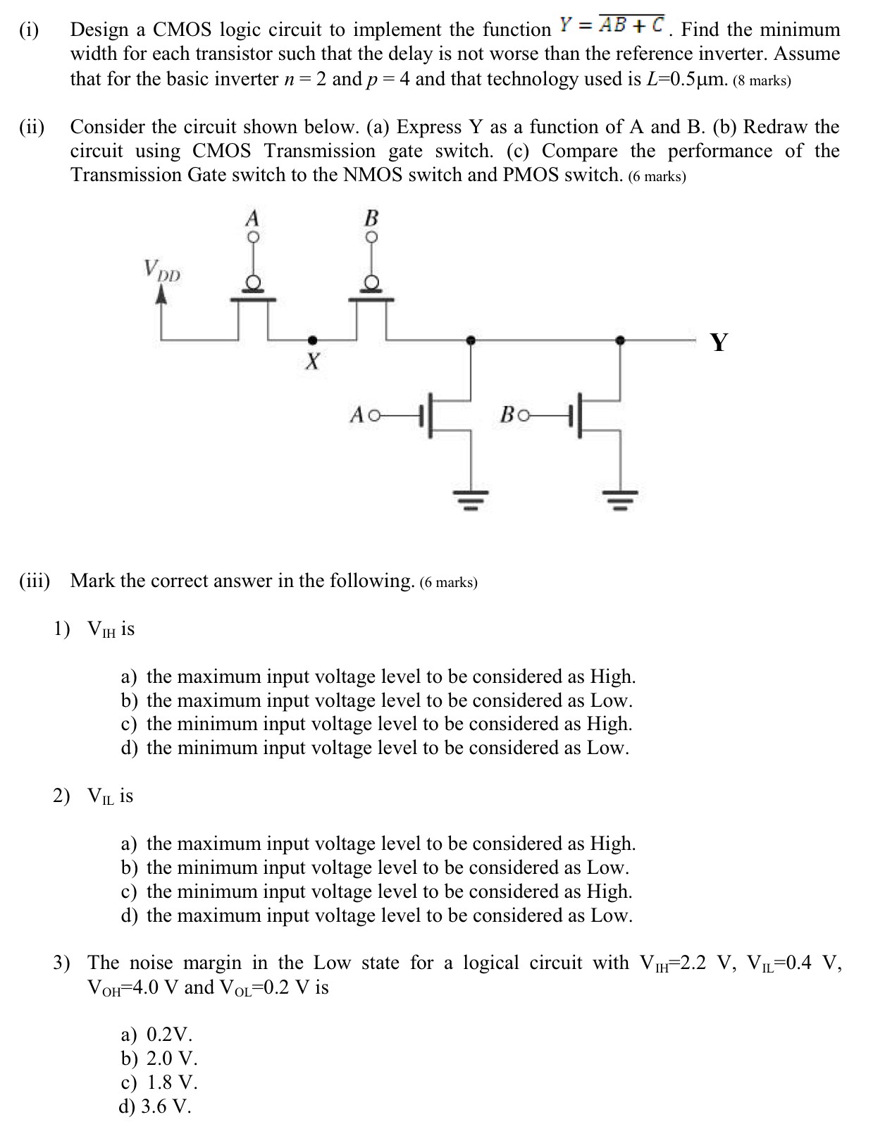
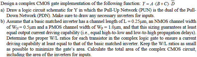
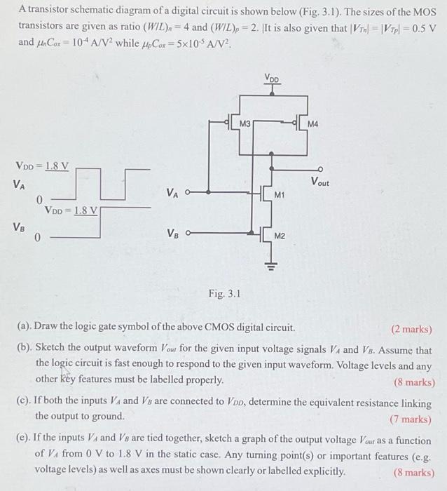
a) Design a CMOS logic circuit to realize the following function Y = A¯B¯C + A¯BC¯ + AB¯C¯ by constructing both the Pull Up Network (PUN) and Pull Down Network (PDN). [6 points] b) Provide the W/L ratios for each transistor in the logic circuit obtained in a). Assume that for the basic inverter n = 2, p = 4 and L = 0.5 μm. [3 points ] c) Design a pass-transistor-logic circuit (transmission gate) to realize the function Y¯ = AB + A¯B¯. [3 points] d) Define the following parameters; and find them from the shown VTC [3 points ] i) VIH ii) VIL iii) NML iv) NMH
![a) Design a CMOS logic circuit to realize the following function Y = A¯B¯C + A¯BC¯ + AB¯C¯ by constructing both the Pull Up Network (PUN) and Pull Down Network (PDN). [6 points] b) Provide the W/L ratios for each transistor in the logic circuit obtained in a). Assume that for the basic inverter n = 2, p = 4 and L = 0.5 μm. [3 points ] c) Design a pass-transistor-logic circuit (transmission gate) to realize the function Y¯ = AB + A¯B¯. [3 points] d) Define the following parameters; and find them from the shown VTC [3 points ] i) VIH ii) VIL iii) NML iv) NMH](https://www.doubtrix.com/uploads/editor/9275382229uigCHoIzXG.jpg)