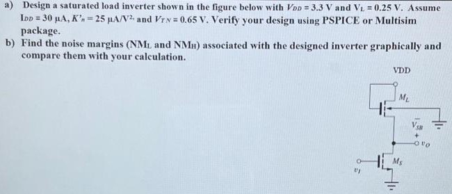
a) Design a saturated load inverter shown in the figure below with VDD = 3.3 V and VL = 0.25 V . Assume IDD = 30 μA, Kn' = 25 μA/V2, and VTN = 0.65 V. Verify your design using PSPICE or Multisim package. b) Find the noise margins (NML and NMH) associated with the designed inverter graphically and compare them with your calculation.

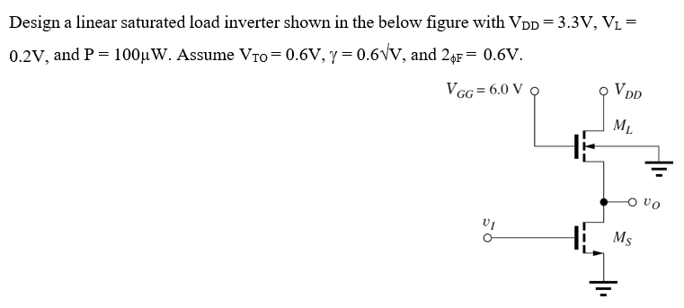
![b. Design the NMOS saturated inverter shown in Figure 3 for VDD = 3.3 V and P = 0.1 mW with Vo = 0.2 V and IDD = 33 μA. Assume Kn′ = 25 μA/V2 and VTN = 1 V. Explain the functionality of the inverter. [5 marks] ii. Design the inverter with the data given above. Ignore the body effect [10 marks] Figure 3](https://www.doubtrix.com/uploads/editor/1774621224JkZBZuRKAk.png)