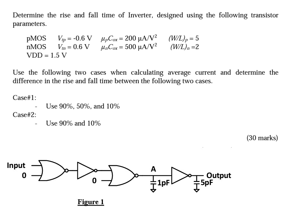
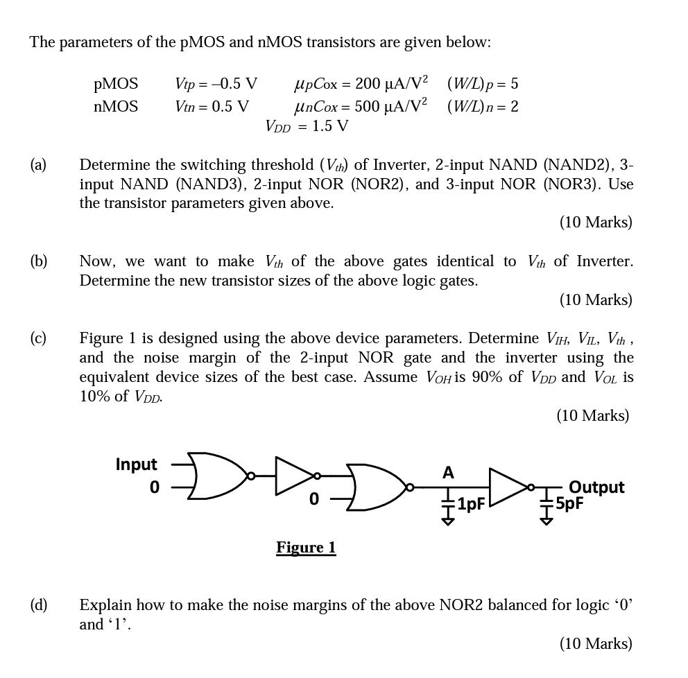
(a) Determine the switching threshold (Vth) of Inverter, 2-input NAND (NAND2), 3input NAND (NAND3), 2-input NOR (NOR2), and 3-input NOR (NOR3). Use the transistor parameters given above. (10 Marks) (b) Now, we want to make Vth of the above gates identical to Vth of Inverter. Determine the new transistor sizes of the above logic gates. (10 Marks) (c) Figure 1 is designed using the above device parameters. Determine VIH, VIL, Vth, and the noise margin of the 2-input NOR gate and the inverter using the equivalent device sizes of the best case. Assume VOH is 90% of VDD and VOL is 10% of VDD. (10 Marks) (d) Explain how to make the noise margins of the above NOR2 balanced for logic ' 0 ' and ' 1 '. (10 Marks) The parameters of the pMOS and nMOS transistors are given below: pMOS Vtp = -0.6 V upCox = 200 uA/V2 (W/L)p = 5 nMOS Vtn = 0.6 V unCox = 500 uA/V2 (W/L)n = 2 VDD = 1.5 V

You'll get a detailed, step-by-step and expert verified solution.
 Work With Experts to Reach at Correct Answers