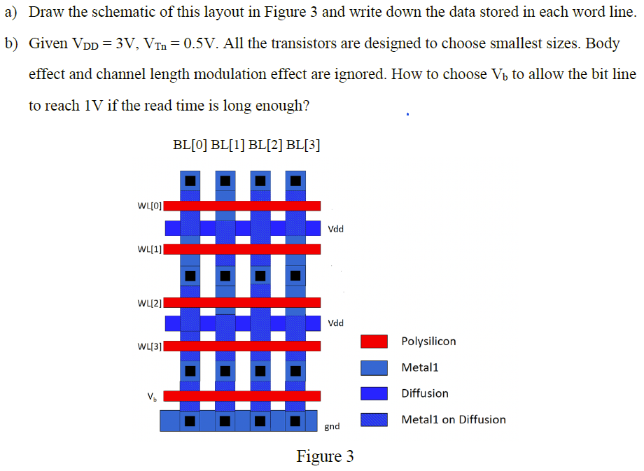
a) Draw the schematic of this layout in Figure 3 and write down the data stored in each word line. b) Given VDD = 3 V, VTn = 0.5 V. All the transistors are designed to choose smallest sizes. Body effect and channel length modulation effect are ignored. How to choose Vb to allow the bit line to reach 1 V if the read time is long enough? Figure 3
a) Draw the schematic of this layout in Figure 3 and write down the data stored in each word line. b) Given VDD = 3 V, VTn = 0.5 V. All the transistors are designed to choose smallest sizes. Body effect and channel length modulation effect are ignored. How to choose Vb to allow the bit line to reach 1 V if the read time is long enough? Figure 3

Image text
a) Draw the schematic of this layout in Figure 3 and write down the data stored in each word line. b) Given V D D = 3 V , V T n = 0.5 V . All the transistors are designed to choose smallest sizes. Body effect and channel length modulation effect are ignored. How to choose V b to allow the bit line to reach 1 V if the read time is long enough? Figure 3

Detailed Answer