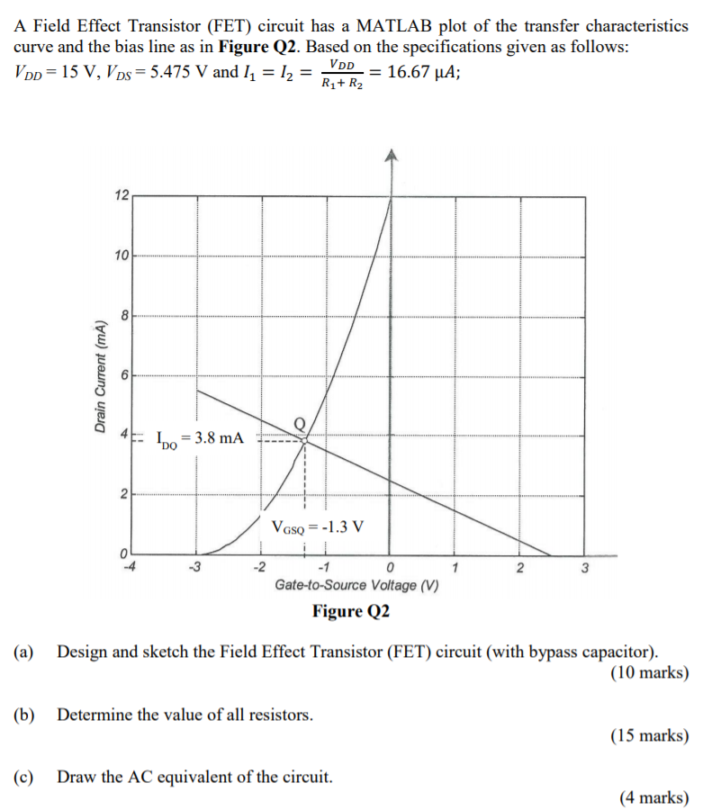
A Field Effect Transistor (FET) circuit has a MATLAB plot of the transfer characteristics curve and the bias line as in Figure Q2. Based on the specifications given as follows: VDD = 15 V, VDS = 5.475 V and I1 = I2 = VDD R1+R2 = 16.67 μA; Figure Q2 (a) Design and sketch the Field Effect Transistor (FET) circuit (with bypass capacitor). (10 marks) (b) Determine the value of all resistors. (15 marks) (c) Draw the AC equivalent of the circuit. (4 marks)