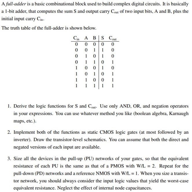
A full-adder is a basic combinational block used to build complex digital circuits. It is basically a 1-bit adder, that computes the sum S and output carry Cout of two input bits, A and B, plus the initial input carry Cin. The truth table of the full-adder is shown below. Cin A B S Cout 0 0 0 0 0 0 0 1 1 0 0 1 0 1 0 0 1 1 0 1 1 0 0 1 0 1 0 1 0 1 1 1 0 0 1 1 1 1 1 1 1. Derive the logic functions for S and Cout. Use only AND, OR, and negation operators in your expressions. You can use whatever method you like (boolean algebra, Karnaugh maps, etc.). 2. Implement both of the functions as static CMOS logic gates (at most followed by an inverter). Draw the transistor-level schematics. You can assume that both the direct and negated versions of each input are available. 3. Size all the devices in the pull-up (PU) networks of your gates, so that the equivalent resistance of each PU is the same as that of a PMOS with W/L = 2. Repeat for the pull-down (PD) networks and a reference NMOS with W/L = 1. When you size a transistor network, you should always consider the input logic values that yield the worst-case equivalent resistance. Neglect the effect of internal node capacitances.
Image text
A full-adder is a basic combinational block used to build complex digital circuits. It is basically a 1-bit adder, that computes the sum S and output carry Cout of two input bits, A and B, plus the initial input carry Cin. The truth table of the full-adder is shown below. Cin A B S Cout 0 0 0 0 0 0 0 1 1 0 0 1 0 1 0 0 1 1 0 1 1 0 0 1 0 1 0 1 0 1 1 1 0 0 1 1 1 1 1 1 1. Derive the logic functions for S and Cout. Use only AND, OR, and negation operators in your expressions. You can use whatever method you like (boolean algebra, Karnaugh maps, etc.). 2. Implement both of the functions as static CMOS logic gates (at most followed by an inverter). Draw the transistor-level schematics. You can assume that both the direct and negated versions of each input are available. 3. Size all the devices in the pull-up (PU) networks of your gates, so that the equivalent resistance of each PU is the same as that of a PMOS with W/L = 2. Repeat for the pull-down (PD) networks and a reference NMOS with W/L = 1. When you size a transistor network, you should always consider the input logic values that yield the worst-case equivalent resistance. Neglect the effect of internal node capacitances.