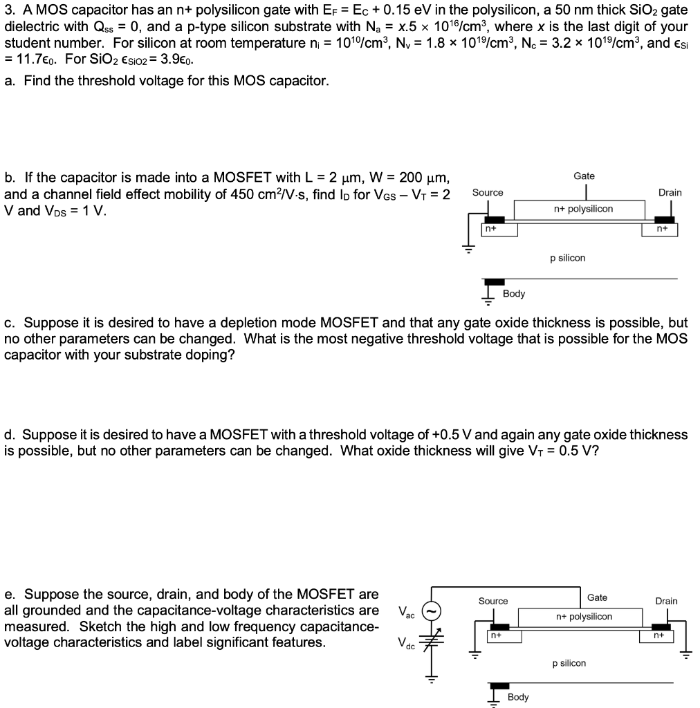
A MOS capacitor has an n+ polysilicon gate with EF = EC+0.15 eV in the polysilicon, a 50 nm thick SiO2 gate dielectric with Qss = 0, and a p-type silicon substrate with Na = x.5×1016 /cm3, where x is the last digit of your student number. For silicon at room temperature ni = 1010 /cm3, Nv = 1.8×10¹⁹ /cm3, Nc = 3.2×10¹⁹ /cm3, and ϵSi = 11.7ϵ0. For SiO2 ϵSiO2 = 3.9ϵ0. a. Find the threshold voltage for this MOS capacitor. b. If the capacitor is made into a MOSFET with L = 2 μm, W = 200 μm, and a channel field effect mobility of 450 cm2/V⋅s, find ID for VGS − VT = 2 V and VDS = 1 V. c. Suppose it is desired to have a depletion mode MOSFET and that any gate oxide thickness is possible, but no other parameters can be changed. What is the most negative threshold voltage that is possible for the MOS capacitor with your substrate doping? d. Suppose it is desired to have a MOSFET with a threshold voltage of +0.5 V and again any gate oxide thickness is possible, but no other parameters can be changed. What oxide thickness will give VT = 0.5 V ? e. Suppose the source, drain, and body of the MOSFET are all grounded and the capacitance-voltage characteristics are measured. Sketch the high and low frequency capacitance-voltage characteristics and label significant features.