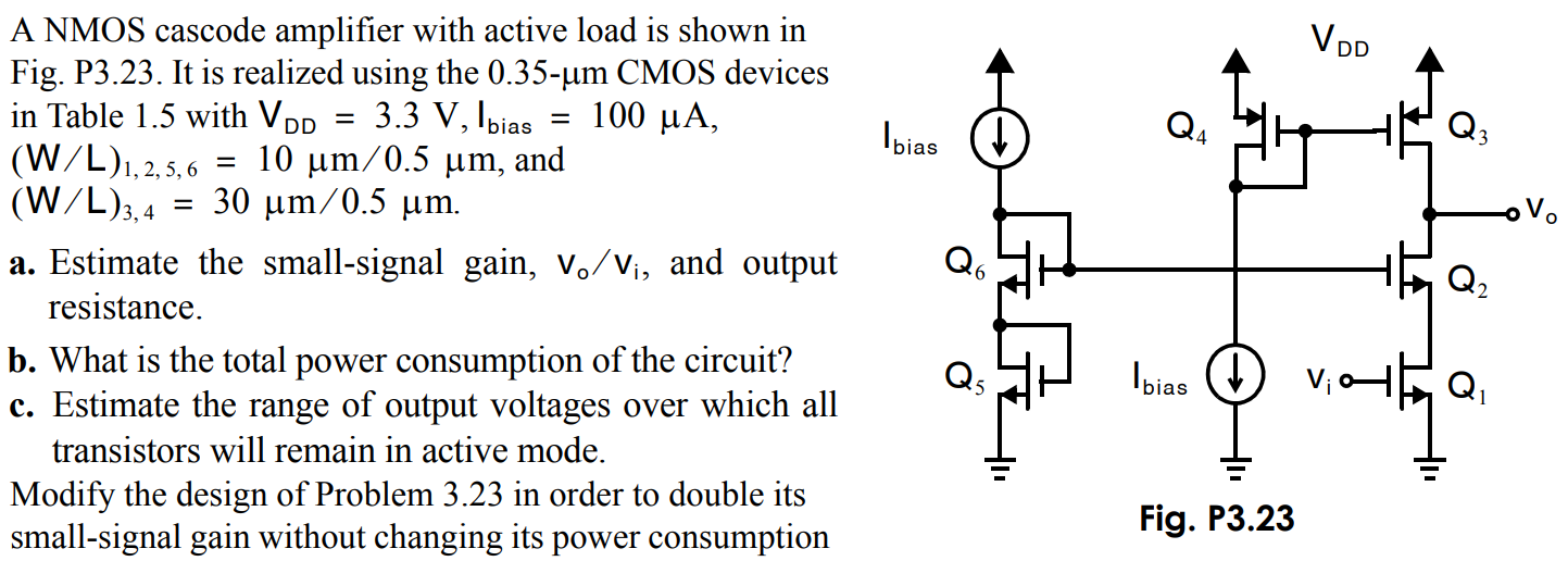
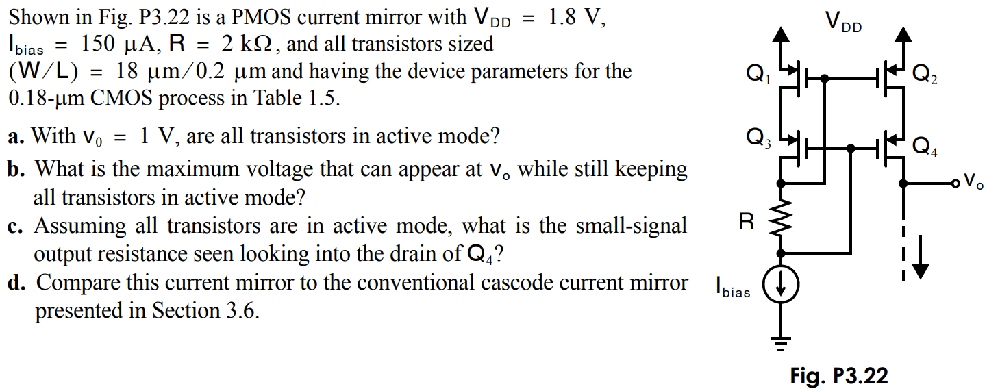
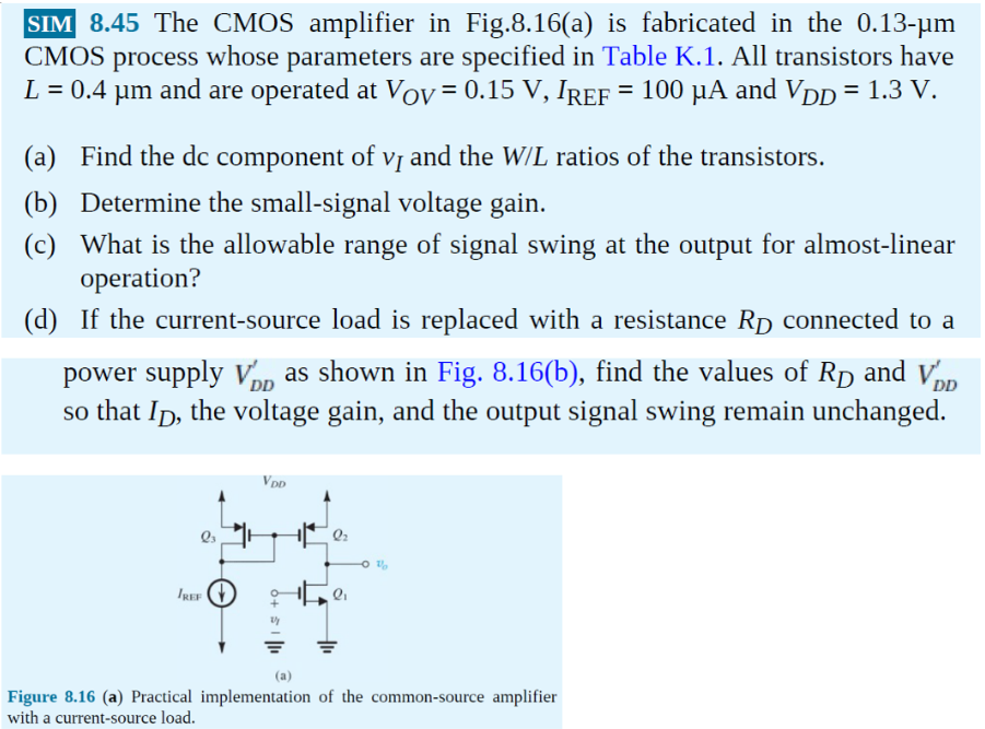
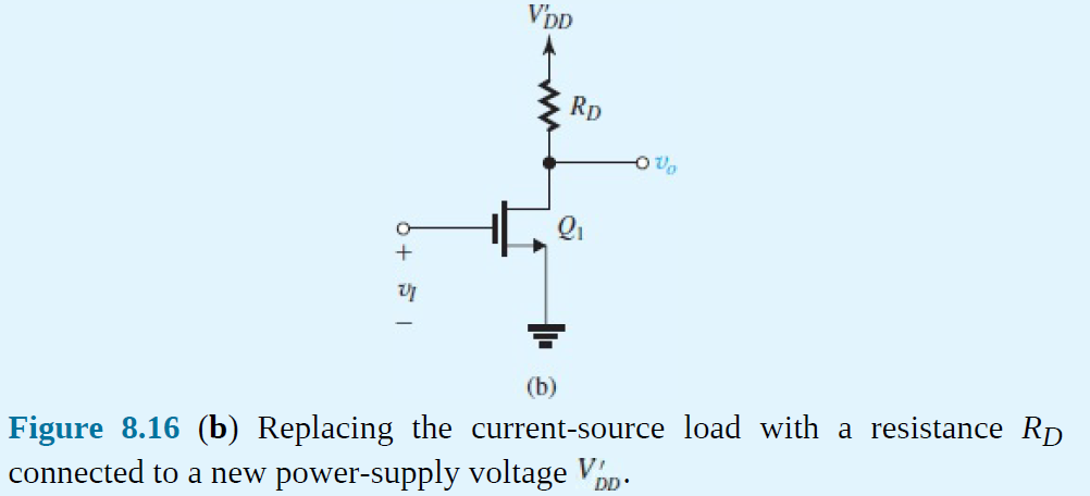
A NMOS cascode amplifier with active load is shown in Fig. P3.23. It is realized using the 0.35-µm CMOS devices in Table 1.5 with VDD = 3.3 V, Ibias = 100 µA, (W/L)1,2,5,6 = 10 µm/0.5 µm, and (W/L)3,4 = 30 µm/0.5 µm. a. Estimate the small-signal gain, vo/vi , and output resistance. b. What is the total power consumption of the circuit? c. Estimate the range of output voltages over which all transistors will remain in active mode. Modify the design of Problem 3.23 in order to double its small-signal gain without changing its power consumption Fig. P3.23
Image text
A NMOS cascode amplifier with active load is shown in Fig. P3.23. It is realized using the 0.35-µm CMOS devices in Table 1.5 with VDD = 3.3 V, Ibias = 100 µA, (W/L)1,2,5,6 = 10 µm/0.5 µm, and (W/L)3,4 = 30 µm/0.5 µm. a. Estimate the small-signal gain, vo/vi , and output resistance. b. What is the total power consumption of the circuit? c. Estimate the range of output voltages over which all transistors will remain in active mode. Modify the design of Problem 3.23 in order to double its small-signal gain without changing its power consumption Fig. P3.23