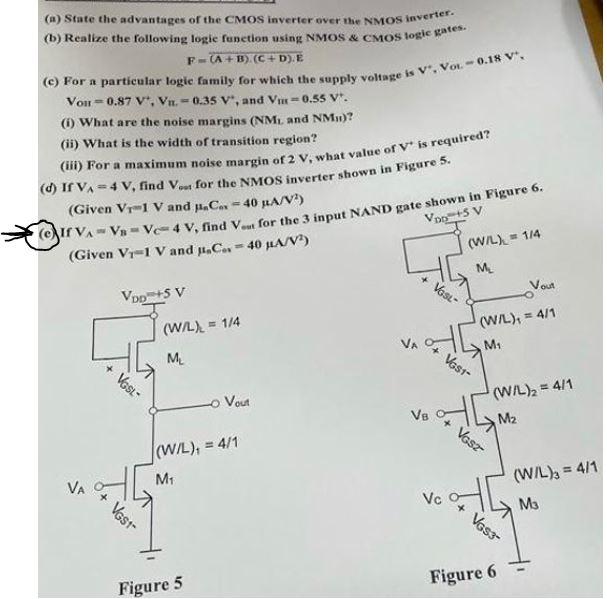
(a) State the advantages of the CMOS inverter over the NMOS inverter. (b) Realize the following logic function using NMOS & CMOs logic gates. F = (A+B).(C+D).E (c) For a particular logic family for which the supply voltage is V+, VOL = 0.18 V+. VOH = 0.87 V+, VIL = 0.35 V+, and VIH = 0.55 V+. (i) What are the noise margins (NML and NMH)? (ii) What is the width of transition region? (iii) For a maximum noise margin of 2 V, what value of V + is required (d) If VA = 4 V, find Vout for the NMOS inverter shown in figure 5. (Given VT = 1 V and μnCox = 40 μA/V2) (e) If VA = VB = VC = 4 V, find Vout for the 3 input NAND gate shown in Figure 6. (Given VT = 1 V and μnCox = 40 μA/V2)
Image text
(a) State the advantages of the CMOS inverter over the NMOS inverter. (b) Realize the following logic function using NMOS & CMOs logic gates. F = (A+B).(C+D).E (c) For a particular logic family for which the supply voltage is V+, VOL = 0.18 V+. VOH = 0.87 V+, VIL = 0.35 V+, and VIH = 0.55 V+. (i) What are the noise margins (NML and NMH)? (ii) What is the width of transition region? (iii) For a maximum noise margin of 2 V, what value of V + is required (d) If VA = 4 V, find Vout for the NMOS inverter shown in figure 5. (Given VT = 1 V and μnCox = 40 μA/V2) (e) If VA = VB = VC = 4 V, find Vout for the 3 input NAND gate shown in Figure 6. (Given VT = 1 V and μnCox = 40 μA/V2)