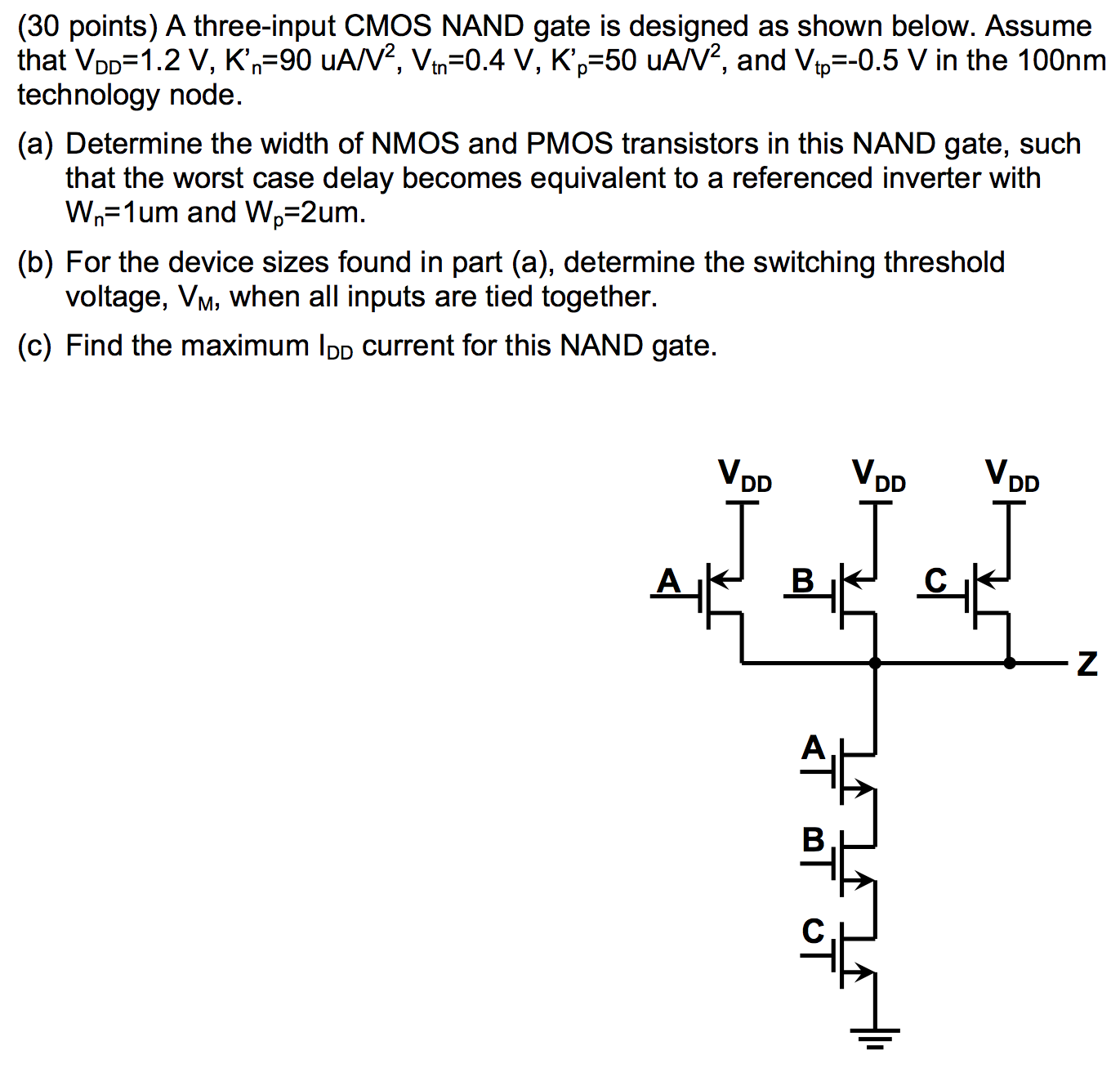
A three-input CMOS NAND gate is designed as shown below. Assume that VDD=1.2 V, K'n = 90 uA/V2, Vtn = 0.4 V, K'p = 50 uA/V2, and Vtp=-0.5 V in the 100nm technology node. Determine the width of NMOS and PMOS transistors in this NAND gate, such that the worst case delay becomes equivalent to a referenced inverter with Wn=1um and Wp=2um. For the device sizes found in part (a), determine the switching threshold voltage, VM, when all inputs are tied together. Find the maximum IDD current for this NAND gate.

You'll get a detailed, step-by-step and expert verified solution.
 Work With Experts to Reach at Correct Answers