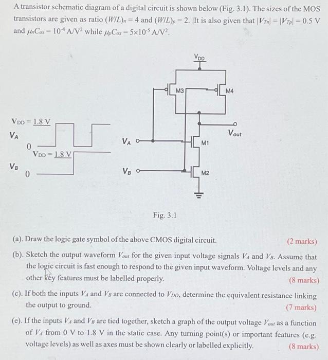
A transistor schematic diagram of a digital circuit is shown below (Fig. 3.1). The sizes of the MOS transistors are given as ratio (W/L)n = 4 and (W/L)p = 2. |It is also given that |VTn| = VTp = 0.5 V and µnCox = 10-4 A/V2 while µpCox = 5 × 10⁻⁵ A/V2 . Fig. 3.1 (a). Draw the logic gate symbol of the above CMOS digital circuit. (2 marks) (b). Sketch the output waveform Vout for the given input voltage signals VA and VB. Assume that the logic circuit is fast enough to respond to the given input waveform. Voltage levels and any other key features must be labelled properly. (8 marks) (c). If both the inputs VA and VB are connected to VDD, determine the equivalent resistance linking the output to ground. (7 marks) (e). If the inputs VA and VB are tied together, sketch a graph of the output voltage Vout as a function of VA from 0 V to 1.8 V in the static case. Any turning point(s) or important features (e.g. voltage levels) as well as axes must be shown clearly or labelled explicitly. (8 marks)
Image text
A transistor schematic diagram of a digital circuit is shown below (Fig. 3.1). The sizes of the MOS transistors are given as ratio (W/L)n = 4 and (W/L)p = 2. |It is also given that |VTn| = VTp = 0.5 V and µnCox = 10-4 A/V2 while µpCox = 5 × 10⁻⁵ A/V2 . Fig. 3.1 (a). Draw the logic gate symbol of the above CMOS digital circuit. (2 marks) (b). Sketch the output waveform Vout for the given input voltage signals VA and VB. Assume that the logic circuit is fast enough to respond to the given input waveform. Voltage levels and any other key features must be labelled properly. (8 marks) (c). If both the inputs VA and VB are connected to VDD, determine the equivalent resistance linking the output to ground. (7 marks) (e). If the inputs VA and VB are tied together, sketch a graph of the output voltage Vout as a function of VA from 0 V to 1.8 V in the static case. Any turning point(s) or important features (e.g. voltage levels) as well as axes must be shown clearly or labelled explicitly. (8 marks)