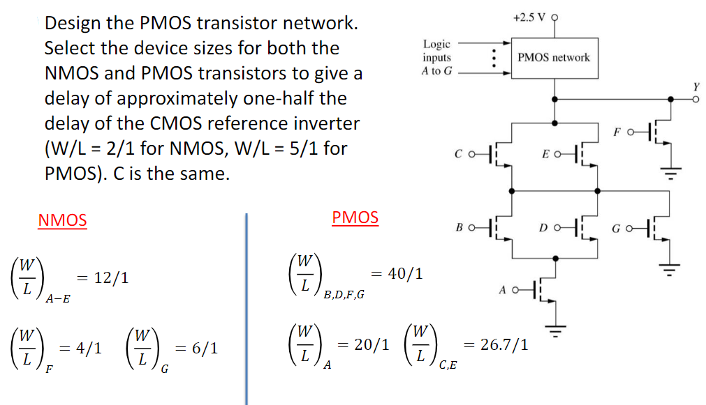
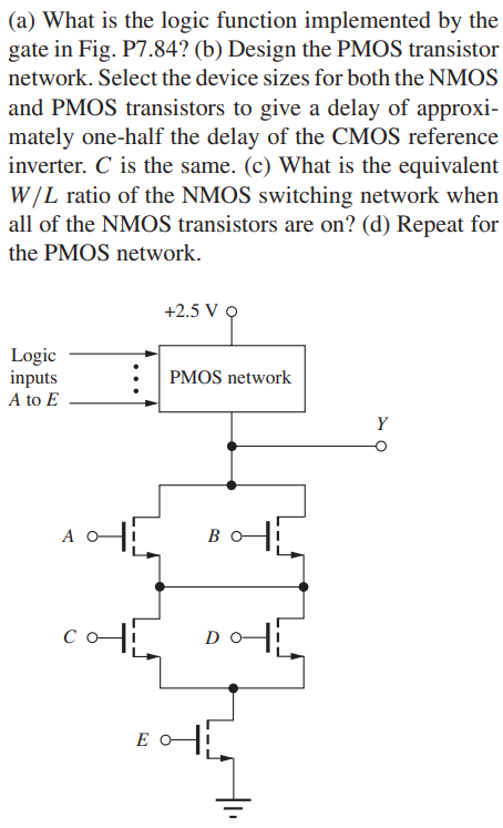
(a) What is the logic function implemented by the gate in Fig. P7.84? (b) Design the PMOS transistor network. Select the device sizes for both the NMOS and PMOS transistors to give a delay of approximately one-half the delay of the CMOS reference inverter. C is the same. (c) What is the equivalent W/L ratio of the NMOS switching network when all of the NMOS transistors are on? (d) Repeat for the PMOS network.

You'll get a detailed, step-by-step and expert verified solution.
 Work With Experts to Reach at Correct Answers