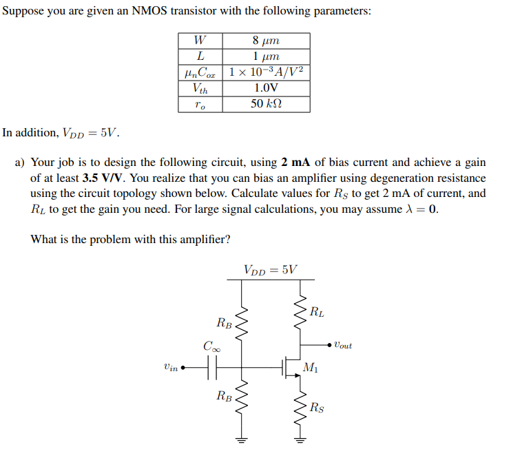
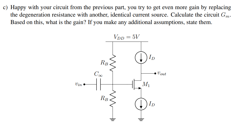
a) Your job is to design the following circuit, using 2 mA of bias current and achieve a gain of at least 3.5 V/V. You realize that you can bias an amplifier using degeneration resistance using the circuit topology shown below. Calculate values for RS to get 2 mA of current, and RL to get the gain you need. For large signal calculations, you may assume lambda = 0. What is the problem with this amplifier? b) You suggest replacing the load resistance RL with a current source that has a very large output impedance, as shown below. The current source requires a headroom of at least 0.5 V. What is the gain of the amplifier? How does this fix the problem from the previous part? 1 Debugging Amplifiers Suppose you are given an NMOS transistor with the following parameters: In addition, VDD = 5 V.

You'll get a detailed, step-by-step and expert verified solution.
 Work With Experts to Reach at Correct Answers