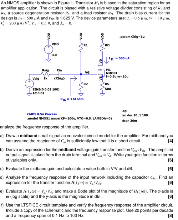
An NMOS amplifier is shown in Figure 1. Transistor M1 is biased in the saturation region for an amplifier application. The circuit is biased with a resistive voltage divider consisting of R1 and R2, a source degeneration resistor RS, and a load resistor RD. The drain bias current for the design is ID = 500 μA and VDS is 1.625 V. The device parameters are: L = 0.5 μm, W = 10 μm, kn’ = 200 μA/V2, Vtn = 0.5 V, and λn = 0. analyze the frequency response of the amplifier. a) Draw a midband small signal ac equivalent circuit model for the amplifier. For midband you can assume the reactance of Cin is sufficiently low that it is a short circuit. b) Derive an expression for the midband voltage gain transfer function Vout /Vsig. The amplified output signal is taken from the drain terminal and Vout = Vd. Write your gain function in terms of variables only. c) Evaluate the midband gain and calculate a value both in V/V and dB. d) Analyze the frequency response of the input network including the capacitor Cin. Find an expression for the transfer function H1(jω) = Vg/Vsig. e) Evaluate H1(jω) = Vg/Vsig and make a Bode plot of the magnitude of H1(jω). The x-axis is ω (log scale) and the y-axis is the magnitude in dB. f) Use the LTSPICE circuit template and verify the frequency response of the amplifier circuit. Include a copy of the schematic and the frequency response plot. Use 20 points per decade and a frequency span of 0.1 Hz to 100 Hz.
Image text
An NMOS amplifier is shown in Figure 1. Transistor M1 is biased in the saturation region for an amplifier application. The circuit is biased with a resistive voltage divider consisting of R1 and R2, a source degeneration resistor RS, and a load resistor RD. The drain bias current for the design is ID = 500 μA and VDS is 1.625 V. The device parameters are: L = 0.5 μm, W = 10 μm, kn’ = 200 μA/V2, Vtn = 0.5 V, and λn = 0. analyze the frequency response of the amplifier. a) Draw a midband small signal ac equivalent circuit model for the amplifier. For midband you can assume the reactance of Cin is sufficiently low that it is a short circuit. b) Derive an expression for the midband voltage gain transfer function Vout /Vsig. The amplified output signal is taken from the drain terminal and Vout = Vd. Write your gain function in terms of variables only. c) Evaluate the midband gain and calculate a value both in V/V and dB. d) Analyze the frequency response of the input network including the capacitor Cin. Find an expression for the transfer function H1(jω) = Vg/Vsig. e) Evaluate H1(jω) = Vg/Vsig and make a Bode plot of the magnitude of H1(jω). The x-axis is ω (log scale) and the y-axis is the magnitude in dB. f) Use the LTSPICE circuit template and verify the frequency response of the amplifier circuit. Include a copy of the schematic and the frequency response plot. Use 20 points per decade and a frequency span of 0.1 Hz to 100 Hz.

![An NMOS amplifier is shown in Figure 1. Transistor M1 is biased in the saturation region for an amplifier application. The circuit is biased with a resistive voltage divider consisting of R1 and R2, a source degeneration resistor RS, and a load resistor RD. The drain bias current for the design is ID = 500 μA and VDS is 1.625 V. The device parameters are: L = 0.5 μm, W = 10 μm, kn′ = 200 μA/V2, Vtn = 0.5 V, and λn = 0. CMOS 0.5 u Process . op . model NMOS1 nmos (KP = 200 u, VTO = 0.5, LAMBDA = 0) ;tran20 m Figure 1: A NMOS amplifier circuit including a source degeneration resistor RS. a) Determine R1 and R2 for the specified bias point. b) Determine the value for RD for the specified bias point. c) Use the LTSPICE circuit template and verify your bias circuit design. Include a copy of the schematic and the dc operating point results (text log with node voltages and currents). [8] d) Use LTSPICE to evaluate the change in ID for a variation in the technology process parameter kn′. Evaluate the change in ID for a change of ±10% in kn′. Compare the relative change in ID with the relative change in kn′. What do you observe? Explain how the source degeneration resistor RS implements negative feedback which reduces the sensitivity of the bias point to changes in kn′. [8]](https://www.doubtrix.com/uploads/editor/9212363628QZkAUhRzqb.jpg)
![For the circuit shown in Figure 1, NMOS device M1 has the following properties: kn’(W/L) = 180 μA/V2, VT0 = 2 V, λ = 0.02 V-1, γ = 0.4 V1/2, 2ϕF = 0.7 V, and ID = 10 mA. Note that capacitor Cbig is a DC blocking cap, i.e., Cbig is an open at DC and a short at all other frequencies. Figure 1. Circuit for Problem 1. a) Determine the numerical value of bias voltage Vbias which is needed to achieve a drain current of ID = 10 mA. b) Draw the small-signal equivalent circuit. c) Analyze the small-signal circuit to find Rin, Rout, and Av = Vout/Vin. Find the analytic expression for each quantity first, before determining the numerical answers. d) Recall that gmb/gm = χ. Determine the numerical value of χ for this problem. [Note that this part has nothing to do with parts (b) and (c).] e) What is the threshold voltage of device M1? [Note that this part has nothing to do with parts (b) and (c).] Show your work, list all numerical values in proper engineering notation format with appropriate units and with at least two decimal places of precision.](https://www.doubtrix.com/js/ckeditor/filemanager/connectors/php/editor/1701531864-Rjgbdog0ehds.png)
![Figure P5-1 shows a common source single transistor MOSFET amplifier utilizing an N-Channel Enhancement Mode MOSFET. The term "common source" refers to the source terminal being shared by both the input circuit and the output circuit. The parameters for the MOSFET and the supply voltage are also given. Hand Analysis P1. In terms of DC bias, determine a value for VGS to set the drain current ID to 5 mA. Also determine a value for RD to set the VDS bias to 6 V. P2. In terms of small-signal parameters, determine the transconductance gm of this amplifier as well as the voltage gain, Av. P3. If vgs is a 0.1 Vpk sinewave at a frequency of 1 kHz [ie. vgs = 0.1sin(2pift)V ] determine an expression for the output voltage vOUT as a function of time. Sketch vIN and vOUT for two complete cycles, including the DC bias for each signal. Simulation P4. Simulate the circuit of Figure P5-1 to verify your hand analysis and create a plot similar to P3 as part of your prelab. Use the virtual MOSFET model in simulation with SPICE parameters VT0 = 1.8 V and KP = 120 mA/V2. (The default values of 100um for W and L will be fine since their ratio equals unity.)](https://www.doubtrix.com/js/ckeditor/filemanager/connectors/php/editor/1695874154-Avjhgifoih.png)