An NMOS device is plugged into the test configuration shown below in Figure 0.4. The input Vin = 2 V. The current source draws a constant current of 50 µA. R is a variable resistor that can assume values between 10 kΩ and 30 kΩ. Transistor M1 experiences short channel effects and has following transistor parameters: k’ = 110*10-6 V/A2, VT = 0.4 , and VDSAT = 0.6V. The transistor has a W/L = 2.5µ/0.25µ. For simplicity body effect and channel length modulation can be neglected. i.e λ=0, γ=0.
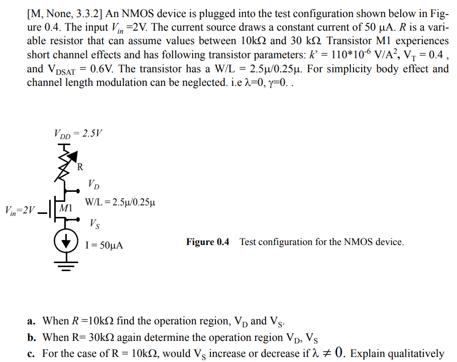
An NMOS device is plugged into the test configuration shown below in Figure 0.4. The input Vin = 2 V. The current source draws a constant current of 50 µA. R is a variable resistor that can assume values between 10 kΩ and 30 kΩ. Transistor M1 experiences short channel effects and has following transistor parameters: k’ = 110*10-6 V/A2, VT = 0.4 , and VDSAT = 0.6V. The transistor has a W/L = 2.5µ/0.25µ. For simplicity body effect and channel length modulation can be neglected. i.e λ=0, γ=0.

Image text
An NMOS device is plugged into the test configuration shown below in Figure 0.4. The input Vin = 2 V. The current source draws a constant current of 50 µA. R is a variable resistor that can assume values between 10 kΩ and 30 kΩ. Transistor M1 experiences short channel effects and has following transistor parameters: k’ = 110*10-6 V/A2, VT = 0.4 , and VDSAT = 0.6V. The transistor has a W/L = 2.5µ/0.25µ. For simplicity body effect and channel length modulation can be neglected. i.e λ=0, γ=0.

Detailed Answer

Answer
  • Student Reviews:
  • (3)
  • Correct answers (3)
  • Complete solution (3)
  • Step-by-step solution (3)
  • Fully explained (3)