Assume the following unless stated otherwise for a 0.25 μm CMOS process: VDD = 5 V, Lmin = 0.25 μm Vtn = 0.5 V or −1 V (choose accordingly), Vtp = −0.5 V μnCox = 265 μA/V2, μpCox = 90 μA/V2 Consider a resistively loaded inverter with a load of Ctot = 300 fF. a) Design the inverter (specify W, L values for the transistor, and RL) so that VOL = 0.025 V. b) Calculate all the other voltages of the voltage transfer characteristic. c) Find the noise margins and the area of the inverter.
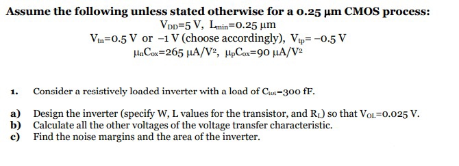
Assume the following unless stated otherwise for a 0.25 μm CMOS process: VDD = 5 V, Lmin = 0.25 μm Vtn = 0.5 V or −1 V (choose accordingly), Vtp = −0.5 V μnCox = 265 μA/V2, μpCox = 90 μA/V2 Consider a resistively loaded inverter with a load of Ctot = 300 fF. a) Design the inverter (specify W, L values for the transistor, and RL) so that VOL = 0.025 V. b) Calculate all the other voltages of the voltage transfer characteristic. c) Find the noise margins and the area of the inverter.

Image text
Assume the following unless stated otherwise for a 0.25 μ m CMOS process:
V D D = 5 V , L min = 0.25 μ m V t n = 0.5 V or 1 V (choose accordingly), V t p = 0.5 V μ n C o x = 265 μ A / V 2 , μ p C o x = 90 μ A / V 2
  1. Consider a resistively loaded inverter with a load of C l v = 300 f F .
    a) Design the inverter (specify W , L values for the transistor, and R L ) so that V O L = 0.025 V .
    b) Calculate all the other voltages of the voltage transfer characteristic.
    c) Find the noise margins and the area of the inverter.

Detailed Answer