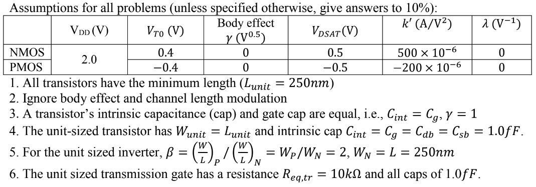
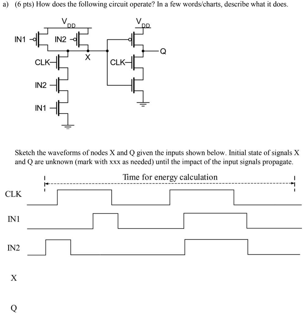
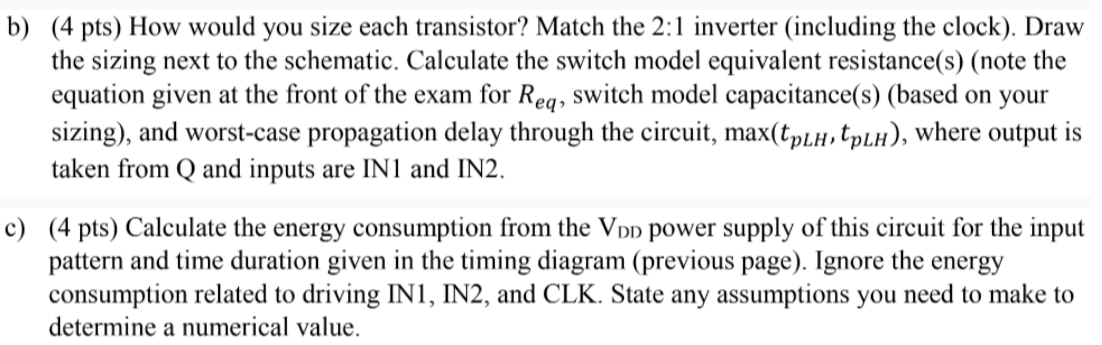
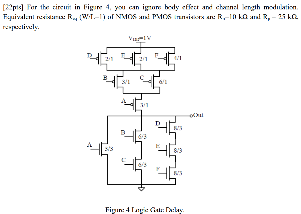
Assumptions for all problems (unless specified otherwise, give answers to 10% ): VDD(V) VT0( V) Body effect γ(V 0.5 ) VDSAT( V) k’ (A/V 2) λ(V -1 ) NMOS 2.0 0.4 0 0.5 500×10-6 0 PMOS -0.4 0 -0.5 -200×10-6 0 1. All transistors have the minimum length (Lunit = 250 nm) 2. Ignore body effect and channel length modulation 3. A transistor's intrinsic capacitance (cap) and gate cap are equal, i.e., Cint = Cg, γ = 1 4. The unit-sized transistor has Wunit = Lunit and intrinsic cap Cint = Cg = Cdb = Csb = 1.0fF. 5. For the unit sized inverter, β = (W/L)P / (W/L N = WP/WN = 2, WN = L = 250 nm 6. The unit sized transmission gate has a resistance Req,tr = 10kΩ and all caps of 1.0fF. a) (6 pts) How does the following circuit operate? In a few words/charts, describe what it does Sketch the waveforms of nodes X and Q given the inputs shown below. Initial state of signals X and Q are unknown (mark with xxx as needed) until the impact of the input signals propagate. X Q b) (4 pts) How would you size each transistor? Match the 2:1 inverter (including the clock). Draw the sizing next to the schematic. Calculate the switch model equivalent resistance(s) (note the equation given at the front of the exam for Req, switch model capacitance(s) (based on your sizing), and worst-case propagation delay through the circuit, max(tpLH,tpLH), where output is taken from Q and inputs are IN1 and IN2. c) (4 pts) Calculate the energy consumption from the VDD power supply of this circuit for the input pattern and time duration given in the timing diagram (previous page). Ignore the energy consumption related to driving IN1, IN2, and CLK. State any assumptions you need to make to determine a numerical value.
Image text
Assumptions for all problems (unless specified otherwise, give answers to 10% ): VDD(V) VT0( V) Body effect γ(V 0.5 ) VDSAT( V) k’ (A/V 2) λ(V -1 ) NMOS 2.0 0.4 0 0.5 500×10-6 0 PMOS -0.4 0 -0.5 -200×10-6 0 1. All transistors have the minimum length (Lunit = 250 nm) 2. Ignore body effect and channel length modulation 3. A transistor's intrinsic capacitance (cap) and gate cap are equal, i.e., Cint = Cg, γ = 1 4. The unit-sized transistor has Wunit = Lunit and intrinsic cap Cint = Cg = Cdb = Csb = 1.0fF. 5. For the unit sized inverter, β = (W/L)P / (W/L N = WP/WN = 2, WN = L = 250 nm 6. The unit sized transmission gate has a resistance Req,tr = 10kΩ and all caps of 1.0fF. a) (6 pts) How does the following circuit operate? In a few words/charts, describe what it does Sketch the waveforms of nodes X and Q given the inputs shown below. Initial state of signals X and Q are unknown (mark with xxx as needed) until the impact of the input signals propagate. X Q b) (4 pts) How would you size each transistor? Match the 2:1 inverter (including the clock). Draw the sizing next to the schematic. Calculate the switch model equivalent resistance(s) (note the equation given at the front of the exam for Req, switch model capacitance(s) (based on your sizing), and worst-case propagation delay through the circuit, max(tpLH,tpLH), where output is taken from Q and inputs are IN1 and IN2. c) (4 pts) Calculate the energy consumption from the VDD power supply of this circuit for the input pattern and time duration given in the timing diagram (previous page). Ignore the energy consumption related to driving IN1, IN2, and CLK. State any assumptions you need to make to determine a numerical value.