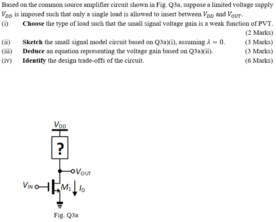
Based on the common source amplifier circuit shown in Fig. Q3a, suppose a limited voltage supply VDD is imposed such that only a single load is allowed to insert between VDD and VOUT. (i) Choose the type of load such that the small signal voltage gain is a weak function of PVT. (2 Marks) (ii) Sketch the small signal model circuit based on Q3a)(i), assuming λ = 0. (3 Marks) (iii) Deduce an equation representing the voltage gain based on Q3a)(ii). (3 Marks) (iv) Identify the design trade-offs of the circuit. (6 Marks)


You'll get a detailed, step-by-step and expert verified solution.
 Work With Experts to Reach at Correct Answers