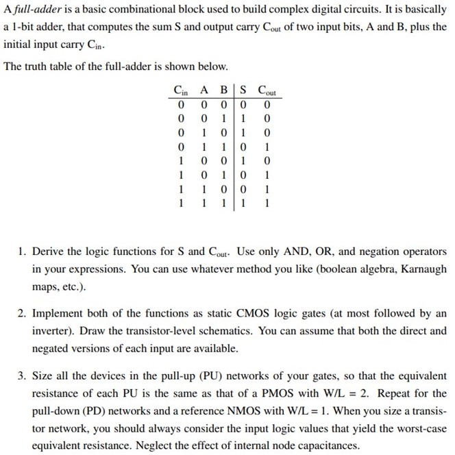
Below is the CMOS diagram of a logic gate that has two inputs A and B and a single output Y. VDD is a logic 1, and ground, represented by a triangle, is a logic 0. a) Fill in the table below. State if P or N-type transistors are ON or OFF, and provide the logic output of Y.

![The circuit shown in Figure 5-1 is a CMOS logic gate of some type. NOTE: Alternative symbols! a) Fill in the table below showing the state of each MOSFET (ON or OFF) and the output voltage for each combination of input states. [10] If 0 V represents a logic low, and +5 V represents a logic high, what is the logic gate function of this circuit? [2] c) Determine the output resistance ROUT of the CMOS gate of Figure 5-1 for each combination of inputs. [8] NOTE: ROUT is the Thevenin Resistance of the Gate. It is the total resistance connected between VDD and the output OR between the output and GROUND, depending on the state of the MOSFET switches. GIVEN : rDSn = 190 ohm and rDSp = 350 ohm d) If this gate exhibits a worst-case Low-to-High (tpLH) propagation delay of 60nsec when driving a given capacitive load, what would you expect the worst-case High-to-Low (tpHL) propagation delay to be?](https://www.doubtrix.com/js/ckeditor/filemanager/connectors/php/editor/1696166621-A78cbckcnnk.png)
![The circuit shown in Figure 5-1 is a CMOS logic gate of some type. NOTE: Alternative symbols! a) Fill in the table below showing the state of each MOSFET (ON or OFF) and the output voltage for each combination of input states. [10] If 0 V represents a logic low, and +5 V represents a logic high, what is the logic gate function of this circuit? [2] c) Determine the output resistance ROUT of the CMOS gate of Figure 5-1 for each combination of inputs. [8] NOTE: ROUT is the Thevenin Resistance of the Gate. It is the total resistance connected between VDD and the output OR between the output and GROUND, depending on the state of the MOSFET switches. GIVEN : rDSn = 190 ohm and rDSp = 350 ohm d) If this gate exhibits a worst-case Low-to-High (tpLH) propagation delay of 60nsec when driving a given capacitive load, what would you expect the worst-case High-to-Low (tpHL) propagation delay to be?](https://www.doubtrix.com/js/ckeditor/filemanager/connectors/php/editor/1696166633-B90cmnnclj.png)