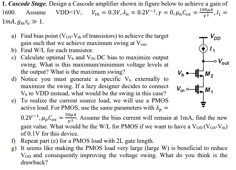
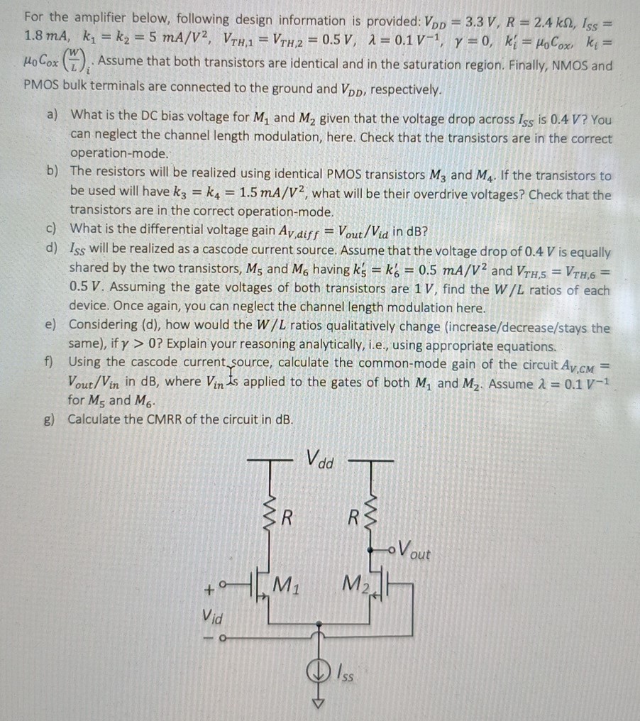
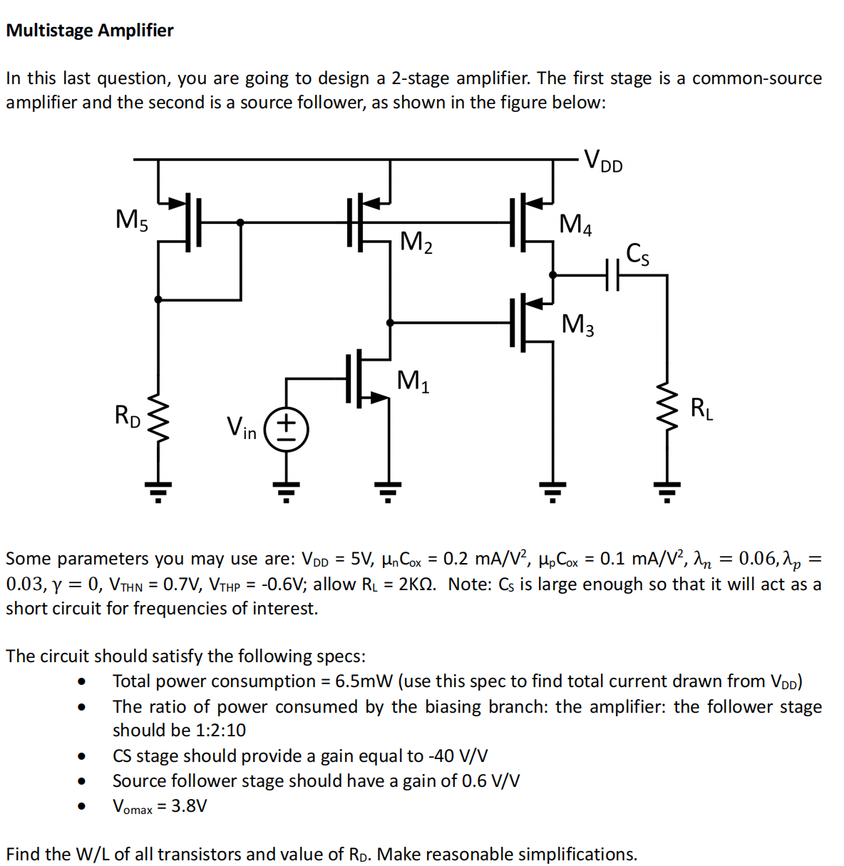
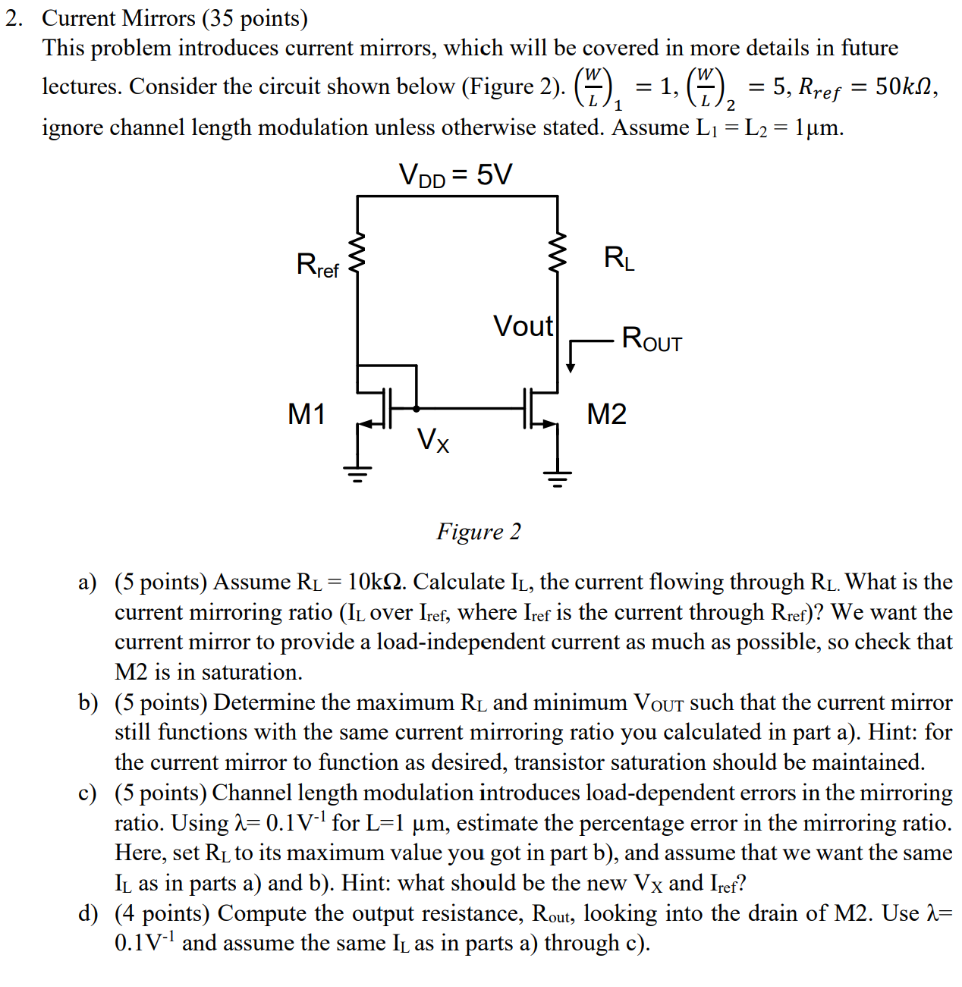
Cascode Stage. Design a Cascode amplifier shown in figure below to achieve a gain of 1600. Assume VDD = 1 V, Vth = 0.3 V, λn = 0.2 V−1, γ = 0, μnCox = 100 μA/V2, I1 = 1 mA, gmro ≫ 1. a) Find bias point (VGS−Vth of transistors) to achieve the target gain such that we achieve maximum swing at Vout. b) Find W/L for each transistor. c) Calculate optimal Vb and VIN DC bias to maximize output swing. What is this maximum/minimum voltage levels at the output? What is the maximum swing? d) Notice you must generate a specific Vb externally to maximize the swing. If a lazy designer decides to connect Vb to VDD instead, what would be the swing in this case? e) To realize the current source load, we will use a PMOS active load. For PMOS, use the same parameters with λp = 0.2 V−1, μpCox = 50 μA/V2. Assume the bias current will remain at 1mA, find the new gain value. What would be the W/L for PMOS if we want to have a VOD(VGS−Vth) of 0.1V for this device. f) Repeat part (e) for a PMOS load with 2L gate length. g) It seems like making the PMOS load very large (large W) is beneficial to reduce VOD and consequently improving the voltage swing. What do you think is the drawback?