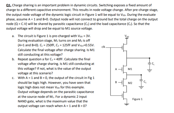
Charge sharing is an important problem in dynamic circuits. Switching exposes a fixed amount of charge to a different capacitive environment. This results in node voltage change. After pre-charge stage, the output node voltage of the dynamic logic circuit in Figure 1 will be equal to VDD. During the evaluate phase, assume A = 1 and B=0. Output node will not connect to ground but the total charge on the output node (Q = C.V) will be shared by parasitic capacitance (C1) and the load capacitance (CL). So that the output voltage will drop and be equal to M1 source voltage.
a. The circuit is Figure 1 is pre-charged with VDD = 3V. During evaluation stage, M1 turns on and M2 is off (A=1 and B=0). CL = 250fF, C1 = 125fF and Vt0,n=0.55V. Calculate the final voltage after charge sharing. Is M1 still conducting at this voltage?
b. Repeat question a for C1 = 40fF. Calculate the final voltage after charge sharing. Is M1 still conducting at this voltage? If not, what is the value of the output voltage at this scenario?
c. With A = 1 and B = 0, the output of the circuit in Fig 1 should be logic high. However, you have seen that logic high does not mean VDD for this example. Output voltage depends on the parasitic capacitance at the source node of M2. For a dynamic 2 input NAND gate, what is the maximum value that the Figure 1 output voltage can reach when A= 1 and B = 0?
Image text
Charge sharing is an important problem in dynamic circuits. Switching exposes a fixed amount of charge to a different capacitive environment. This results in node voltage change. After pre-charge stage, the output node voltage of the dynamic logic circuit in Figure 1 will be equal to VDD. During the evaluate phase, assume A = 1 and B=0. Output node will not connect to ground but the total charge on the output node (Q = C.V) will be shared by parasitic capacitance (C1) and the load capacitance (CL). So that the output voltage will drop and be equal to M1 source voltage.
a. The circuit is Figure 1 is pre-charged with VDD = 3V. During evaluation stage, M1 turns on and M2 is off (A=1 and B=0). CL = 250fF, C1 = 125fF and Vt0,n=0.55V. Calculate the final voltage after charge sharing. Is M1 still conducting at this voltage?
b. Repeat question a for C1 = 40fF. Calculate the final voltage after charge sharing. Is M1 still conducting at this voltage? If not, what is the value of the output voltage at this scenario?
c. With A = 1 and B = 0, the output of the circuit in Fig 1 should be logic high. However, you have seen that logic high does not mean VDD for this example. Output voltage depends on the parasitic capacitance at the source node of M2. For a dynamic 2 input NAND gate, what is the maximum value that the Figure 1 output voltage can reach when A= 1 and B = 0?


![Consider the open-loop circuit (on the left) and closed-loop circuit (on the right) shown in Figure 1 below. In this problem, the open-loop circuit (on the left) will be used to analyze the open-loop behavior of the closed-loop circuit (on the right). closed - loof ciruit Figure 1. Open-loop (left) and closed-loop (right) circuits for Problem 1. Here are the problem parameters:The NMOS devices have gmn = 6 mA/V and rdsn = 25 kΩ. The PMOS devices have gmp = 3 mA/V and rdsp = 15 kΩ. Resistor values are R1 = 1 kΩ and R2 = 3 kΩ. a) Referring to the open-loop circuit of Figure 1, determine the numerical open-loop gain Av. OL = Vout /Vin . For the purposes of this analysis, as we have done a million times before (reminder: this is the 2 nd semester of electronics, so this should not be your first electronics rodeo), you should deactivate all sources in the circuit, except Vin. . b) Referring to the open-loop circuit of Figure 1, determine the numerical open-loop output resistance Rout, oL. , i. e. , the resistance seen looking in at the output node Vout. . You should deactivate all sources in the circuit; feel free to add an appropriate test source(s), if you think you need to do that. c) Referring to the open-loop circuit of Figure 1, determine the numerical loop gain from the test source to the output node: LG = |Vout /Vtest | For the purposes of this analysis, you should deactivate all sources in the circuit, except Vtest. . Also, note that the way the loop gain is defined, it will be a positive-valued quantity. Explain why we want to use a positive loop gain for determining the closed-loop performance [see, e. g. , parts (d) and (e) below]. Your answer for this part should be both i) specific to this problem and ii) generalized to any closed-loop circuit with negative feedback. You are strongly encouraged to consider incorporating a generalized block diagram to help strengthen your argument(s). d) Referring to the closed-loop circuit of Figure 1, determine the numerical closed-loop gain Av, CL = Vout /Vin . Rather than solving the closed-loop circuit of Figure 1 directly for the closed-loop gain, you should instead utilize the results of the previous parts to determine Av, cL. Here, I need to remind you that you should do as you have been (hopefully) doing on the previous parts: first, state the equation you will use to determine Av, cL in terms of, e. g. , Av. ol. and/or Rout, ol and/or LG (i. e. , resist the temptation to dive straight into the numerical values, but feel free to write your equation in terms of Av, ol and/or Rout, ol. and/or LG instead of gmn, gmp, rdsn, rdpp , R1, R2 ), and then plug the numbers in to your equation, and then box your numerical answer along with all the things that we have expected of your numerical quantities since day one. Make it really easy for me to find the equation you used (same story for all of the parts of this problem). e) Referring to the closed-loop circuit of Figure 1, determine the numerical closed-loop output resistance Rout, CL. Rather than solving the closed-loop circuit of Figure 1 directly for the closed-loop output resistance, you should instead follow the same guidance that was given for part (d) of this problem.](https://www.doubtrix.com/uploads/editor/5672518564OTwrDIyJcJ.jpg)