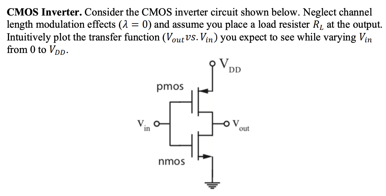
CMOS Inverter. Consider the CMOS inverter circuit shown below. Neglect channel length modulation effects (λ = 0) and assume you place a load resister RL at the output. Intuitively plot the transfer function (Vout vs. Vin) you expect to see while varying Vin from 0 to VDD.
CMOS Inverter. Consider the CMOS inverter circuit shown below. Neglect channel length modulation effects (λ = 0) and assume you place a load resister RL at the output. Intuitively plot the transfer function (Vout vs. Vin) you expect to see while varying Vin from 0 to VDD.

Image text
CMOS Inverter. Consider the CMOS inverter circuit shown below. Neglect channel length modulation effects ( λ = 0 ) and assume you place a load resister R L at the output. Intuitively plot the transfer function ( V out v s . V in ) you expect to see while varying V in from 0 to V D D .

Detailed Answer