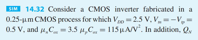
Consider a CMOS inverter fabricated in a 65 nm process that has the following characteristics:
VDD = 2.5V VTn = -VTp = 0.5 V
unCOX = 3.5upCOX = 115 uA/V2
QN & QP -> L = 250 nm & (W/L)N = 1.5
(a) For when WP = 3.5WN (matched case), calculate VM, NML, NMH, and the silicon area used.
(b) For when WP = WN, calculate VM, NML, NMH, and the silicon area used.
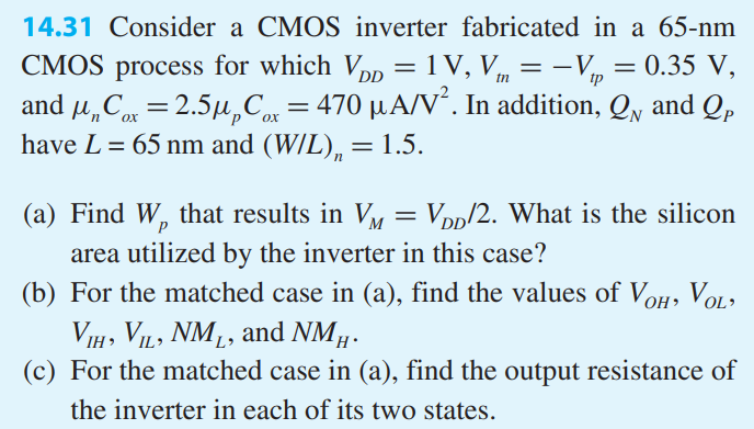
Image text
Consider a CMOS inverter fabricated in a 65 nm process that has the following characteristics:
VDD = 2.5V VTn = -VTp = 0.5 V
unCOX = 3.5upCOX = 115 uA/V2
QN & QP -> L = 250 nm & (W/L)N = 1.5
(a) For when WP = 3.5WN (matched case), calculate VM, NML, NMH, and the silicon area used.
(b) For when WP = WN, calculate VM, NML, NMH, and the silicon area used.