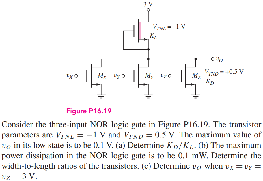
Consider a four-input NMOS NOR logic gate with a depletion load similar to the circuit in Figure P16.19. Assume VDD = 2.5 V, VTND = 0.4 V, and VTNL = −0.6 V. The maximum value of vO in its low state is to be 50 mV. (a) Determine KD/KL. (b) The maximum power dissipation in this NOR logic gate is to be 50 μW. Determine the width-to-length ratio of each transistor. (c) Determine vO when (i) two inputs are a logic 1, (ii) three inputs are a logic 1, and (iii) all inputs are a logic 1. Figure P16.19