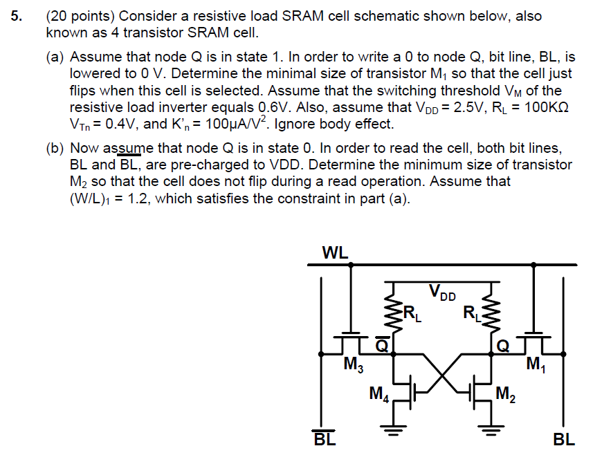
Consider a resistive load SRAM cell schematic shown below, also known as 4 transistor SRAM cell. (a) Assume that node Q is in state 1 . In order to write a 0 to node Q, bit line, BL, is lowered to 0 V. Determine the minimal size of transistor M1 so that the cell just flips when this cell is selected. Assume that the switching threshold VM of the resistive load inverter equals 0.6 V. Also, assume that VDD = 2.5 V, RL = 100 KΩ VTn = 0.4 V, and Kn = 100 μA/V2. Ignore body effect. (b) Now assume that node Q is in state 0 . In order to read the cell, both bit lines, BL and BL, are pre-charged to VDD. Determine the minimum size of transistor M2 so that the cell does not flip during a read operation. Assume that (W/L)1 = 1.2, which satisfies the constraint in part (a).

![[DRAM Analysis] Figure 4 shows a 1 μm×1 μm DRAM cell with NMOS width W = 0.5 μm and CS = 55 fF. Assume VDD = 1 V. Assume that for the NMOS transistor, CD = CG = 1 fF/μm, VTH = 0.2 V, Ileak, n = 1 nA for a W = 0.5 μm device. The cell is arranged in a 128×8 memory block and the wordline and bitline wires have a capacitance of CW = 0.2 fF/μm (i. e. 0.2 fF per unit length). Each bitline is connected to a sense amplifier with ΔVsense = 100 mV and input capacitance 5 fF, and you may ignore loading from any other peripheral circuitry. Use the ideal switch model for the transistor. Figure 4 (a) WRITE: Assume the cell initially stores a " 0 ". In order to write a "1", BL and WL are raised to VDD. What is the final value on node X ? (b) READ: After storing values in your memory, you pre-charge the bitline to VDD/2 and read. What is the final value on the bitline when you are reading a " 1 "?](https://www.doubtrix.com/uploads/editor/7753781189DiGpmnQIJq.png)