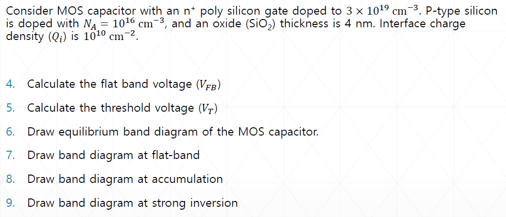
Consider MOS capacitor with an n+poly silicon gate doped to 3×1019 cm−3. P-type silicon is doped with NA = 1016 cm−3, and an oxide (SiO2) thickness is 4 nm. Interface charge density (Qi) is 1010 cm−2.4. Calculate the flat band voltage (VFB) 5. Calculate the threshold voltage (VT) 6. Draw equilibrium band diagram of the MOS capacitor. 7. Draw band diagram at flat-band 8. Draw band diagram at accumulation 9. Draw band diagram at strong inversion
Consider MOS capacitor with an n+poly silicon gate doped to 3×1019 cm−3. P-type silicon is doped with NA = 1016 cm−3, and an oxide (SiO2) thickness is 4 nm. Interface charge density (Qi) is 1010 cm−2.4. Calculate the flat band voltage (VFB) 5. Calculate the threshold voltage (VT) 6. Draw equilibrium band diagram of the MOS capacitor. 7. Draw band diagram at flat-band 8. Draw band diagram at accumulation 9. Draw band diagram at strong inversion

Image text
Consider MOS capacitor with an n + poly silicon gate doped to 3 × 10 19 c m 3 . P-type silicon is doped with N A = 10 16 c m 3 , and an oxide ( S i O 2 ) thickness is 4 n m . Interface charge density ( Q i ) is 10 10 c m 2 . 4. Calculate the flat band voltage ( V F B ) 5. Calculate the threshold voltage ( V T ) 6. Draw equilibrium band diagram of the MOS capacitor. 7. Draw band diagram at flat-band 8. Draw band diagram at accumulation 9. Draw band diagram at strong inversion

Detailed Answer