Consider the circuit in figure. The bias current in the circuit is 0.3 mA and the transistors are biased such that, |Vovn| = 0.5∗|Vovp| = 150 mV. The technology parameters are given by VDD = 1.8 V, |VAp| = 2|VAn| = 12 V. Fill in the table with proper units. Neglect channel length modulation for biasing calculations. (2+4+4+2) Effective small-signal transconductance of the amplifier Small-signal input resistance of the amplifier Small-signal output resistance of the amplifier Small-signal open circuit voltage gain
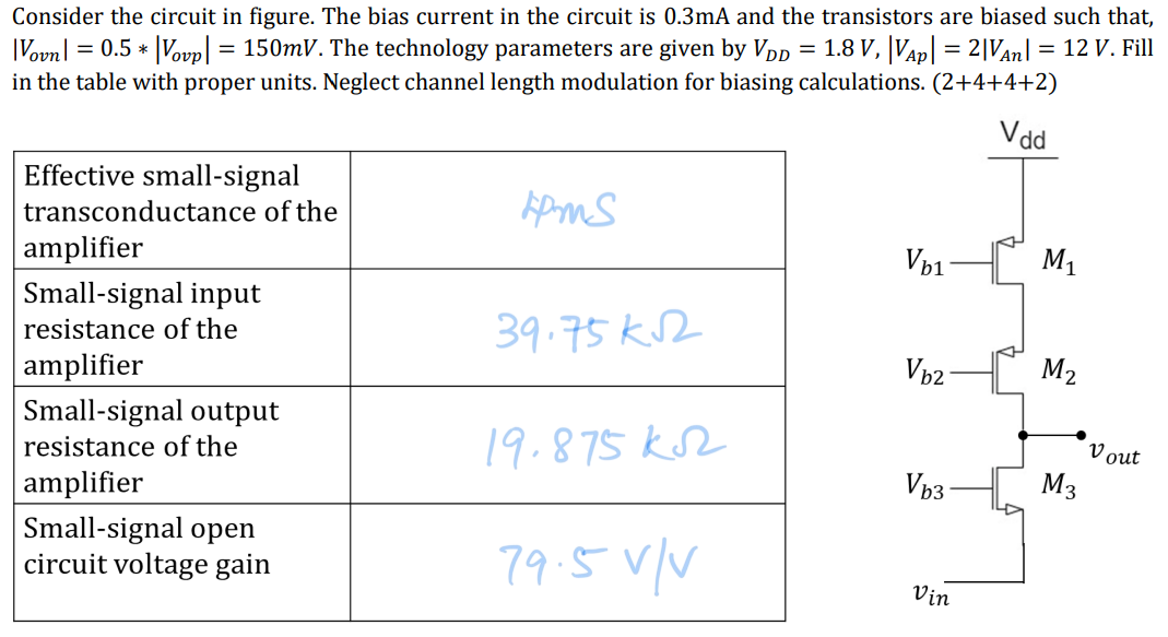
Consider the circuit in figure. The bias current in the circuit is 0.3 mA and the transistors are biased such that, |Vovn| = 0.5∗|Vovp| = 150 mV. The technology parameters are given by VDD = 1.8 V, |VAp| = 2|VAn| = 12 V. Fill in the table with proper units. Neglect channel length modulation for biasing calculations. (2+4+4+2) Effective small-signal transconductance of the amplifier Small-signal input resistance of the amplifier Small-signal output resistance of the amplifier Small-signal open circuit voltage gain

Image text
Consider the circuit in figure. The bias current in the circuit is 0.3 m A and the transistors are biased such that, | V ovn | = 0.5 | V ovp | = 150 m V . The technology parameters are given by V D D = 1.8 V , | V A p | = 2 | V A n | = 12 V . Fill in the table with proper units. Neglect channel length modulation for biasing calculations. ( 2 + 4 + 4 + 2 )

Detailed Answer