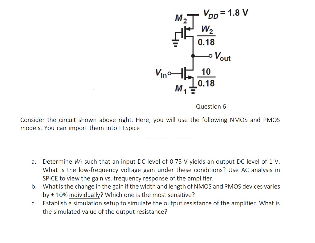
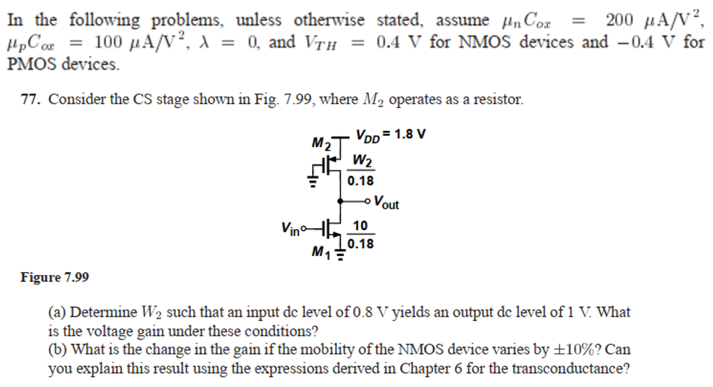
Consider the circuit shown above right. Here, you will use the following NMOS and PMOS models. You can import them into LTSpice a. Determine W2 such that an input DC level of 0.75 V yields an output DC level of 1 V. What is the low-frequency voltage gain under these conditions? Use AC analysis in SPICE to view the gain vs. frequency response of the amplifier. b. What is the change in the gain if the width and length of NMOS and PMOS devices varies by ±10% individually? Which one is the most sensitive? c. Establish a simulation setup to simulate the output resistance of the amplifier. What is the simulated value of the output resistance?
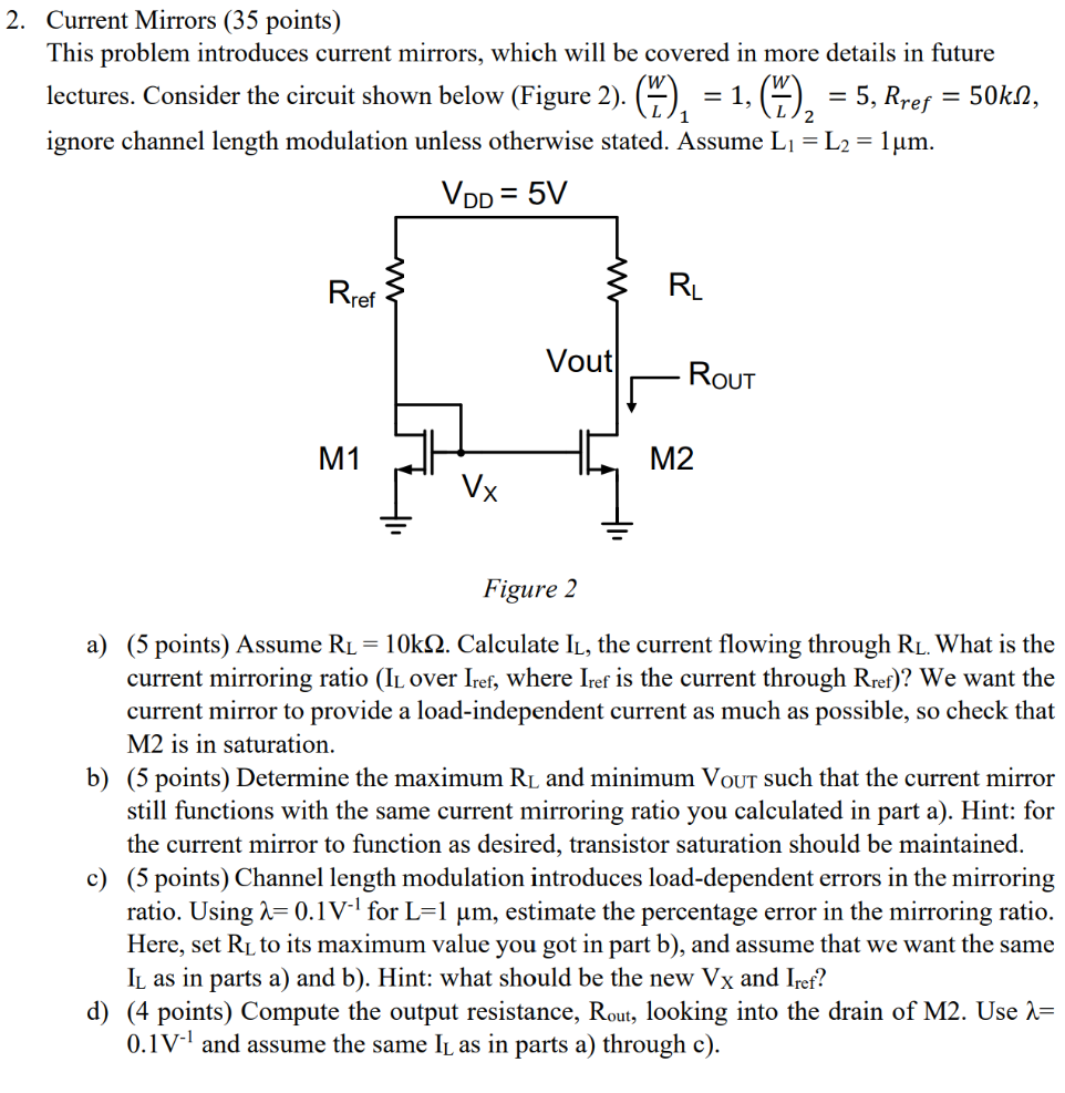
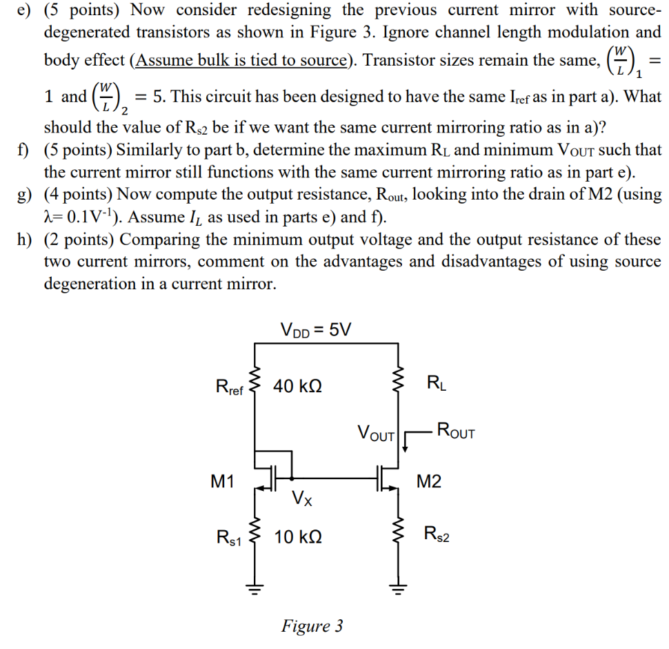
Image text
Consider the circuit shown above right. Here, you will use the following NMOS and PMOS models. You can import them into LTSpice a. Determine W2 such that an input DC level of 0.75 V yields an output DC level of 1 V. What is the low-frequency voltage gain under these conditions? Use AC analysis in SPICE to view the gain vs. frequency response of the amplifier. b. What is the change in the gain if the width and length of NMOS and PMOS devices varies by ±10% individually? Which one is the most sensitive? c. Establish a simulation setup to simulate the output resistance of the amplifier. What is the simulated value of the output resistance?