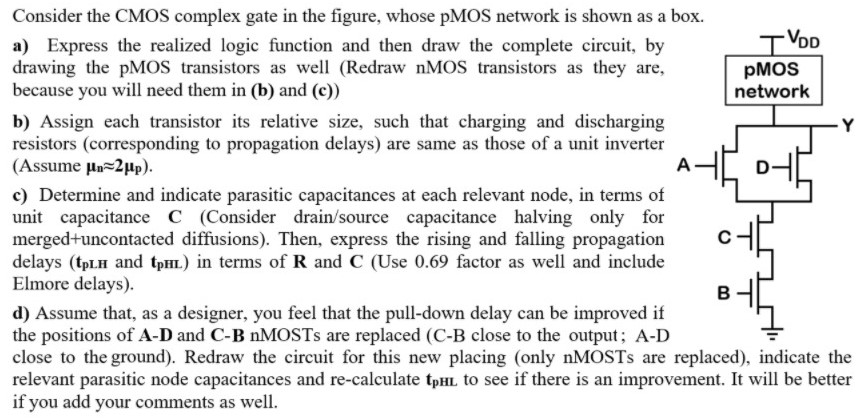
Consider the CMOS complex gate in the figure, whose pMOS network is shown as a box. a) Express the realized logic function and then draw the complete circuit, by drawing the pMOS transistors as well (Redraw nMOS transistors as they are, because you will need them in (b) and (c)) b) Assign each transistor its relative size, such that charging and discharging resistors (corresponding to propagation delays) are same as those of a unit inverter (Assume μn ≈ 2μp ). c) Determine and indicate parasitic capacitances at each relevant node, in terms of unit capacitance C (Consider drain/source capacitance halving only for merged+uncontacted diffusions). Then, express the rising and falling propagation delays ( tpLH and tpHL ) in terms of R and C (Use 0.69 factor as well and include Elmore delays). d) Assume that, as a designer, you feel that the pull-down delay can be improved if the positions of A−D and C-B nMOSTs are replaced (C-B close to the output; A-D close to the ground). Redraw the circuit for this new placing (only nMOSTs are replaced), indicate the relevant parasitic node capacitances and re-calculate tpHL to see if there is an improvement. It will be better if you add your comments as well.