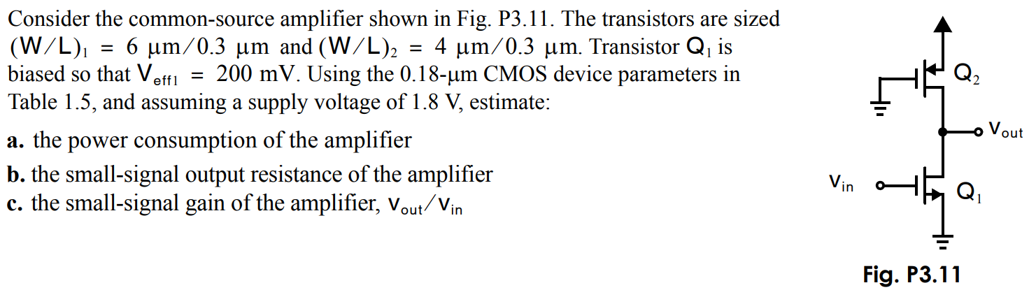
Consider the common-source amplifier shown in Fig. P3.11. The transistors are sized (W/L)1 = 6 µm/0.3 µm and (W/L)2 = 4 µm/0.3 µm. Transistor Q1 is biased so that Veff1 = 200 mV. Using the 0.18−µm CMOS device parameters in Table 1.5, and assuming a supply voltage of 1.8 V, estimate: a. the power consumption of the amplifier b. the small-signal output resistance of the amplifier c. the small-signal gain of the amplifier, vout /vin


You'll get a detailed, step-by-step and expert verified solution.
 Work With Experts to Reach at Correct Answers
![Consider the following amplifier circuit. Both MOSFET’s have the following specifications: (W/L) = (6µm/0.18µm), processing parameters kp = µpCox = 70µA/V2 , kn = µnCox = 270µA/V2 , |Vt| = 0.45 V, V Ω A = 12.5 V/µm = VA, and Q1 is biased so that Vov = 200mV, gate of Q2 is at DC voltage VG = 0.96 V and VDD = 1.8 V. a. What is the configuration of amplifier, i.e. CE or CB or CD or CS or CG or CC or CD or CS with active load or CG with active load or CE with active load or CB with active load or CD with active load or CC with active load or CE using 0.18µm technology? Or none of the above the correct answer is b. Find the small-signal output resistance Rout and input resistance Rin looking into gate Q1 c. Calculate small-signal voltage gain of the amplifier Av = [vo/vi ] d. What is the voltage swing at the output, i.e. vomax and vomin ? e. Calculate the power consumed by the amplifier.](https://www.doubtrix.com/uploads/editor/9038008426JohCcjsvNB.jpg)