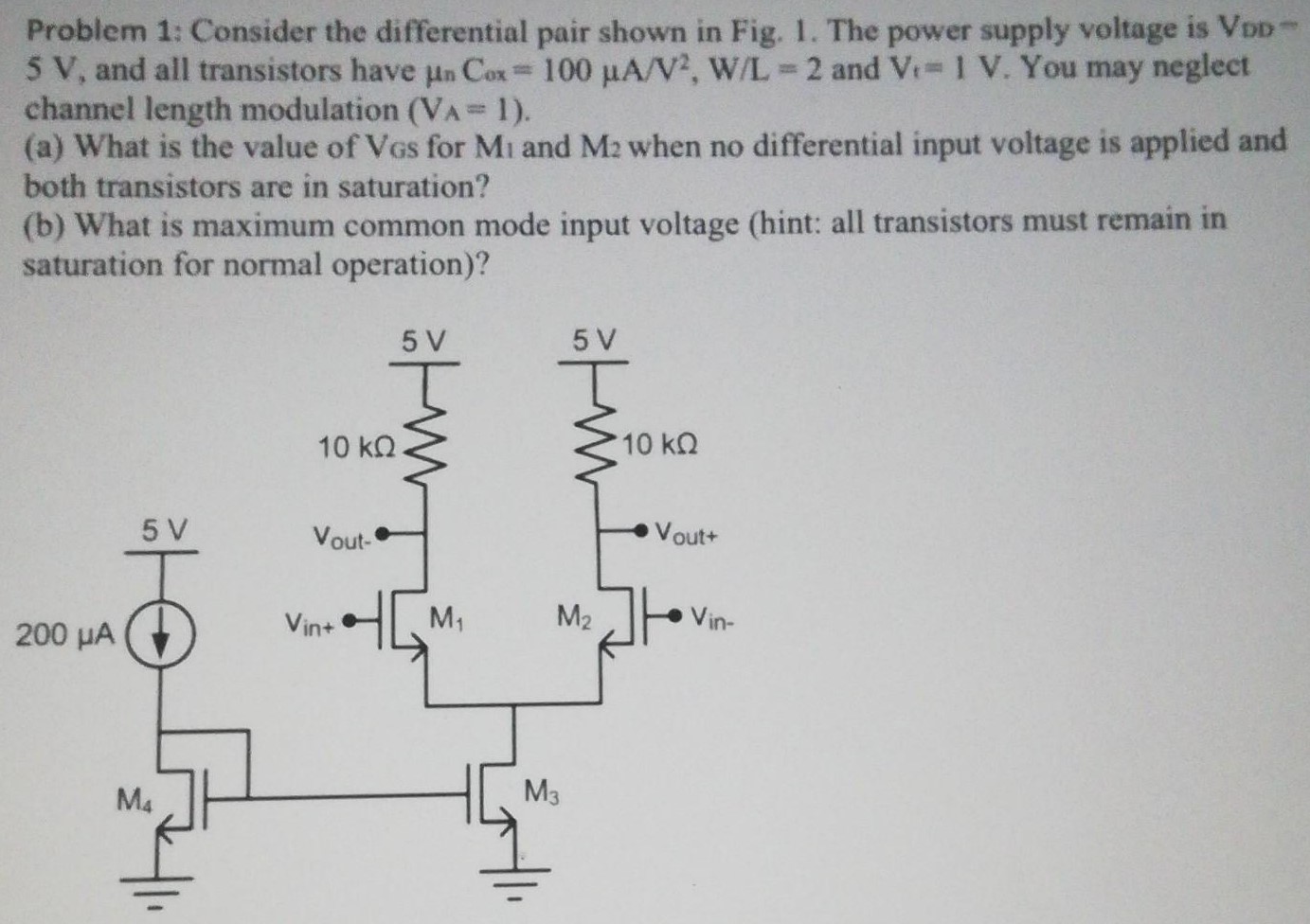
Consider the differential pair shown in Fig. 1. The power supply voltage is VDD 5 V, and all transistors have μnCox = 100 μA/V2, W/L = 2 and Vt = 1 V. You may neglect channel length modulation (VA = 1). (a) What is the value of VGS for M1 and M2 when no differential input voltage is applied and both transistors are in saturation? (b) What is maximum common mode input voltage (hint: all transistors must remain in saturation for normal operation)?
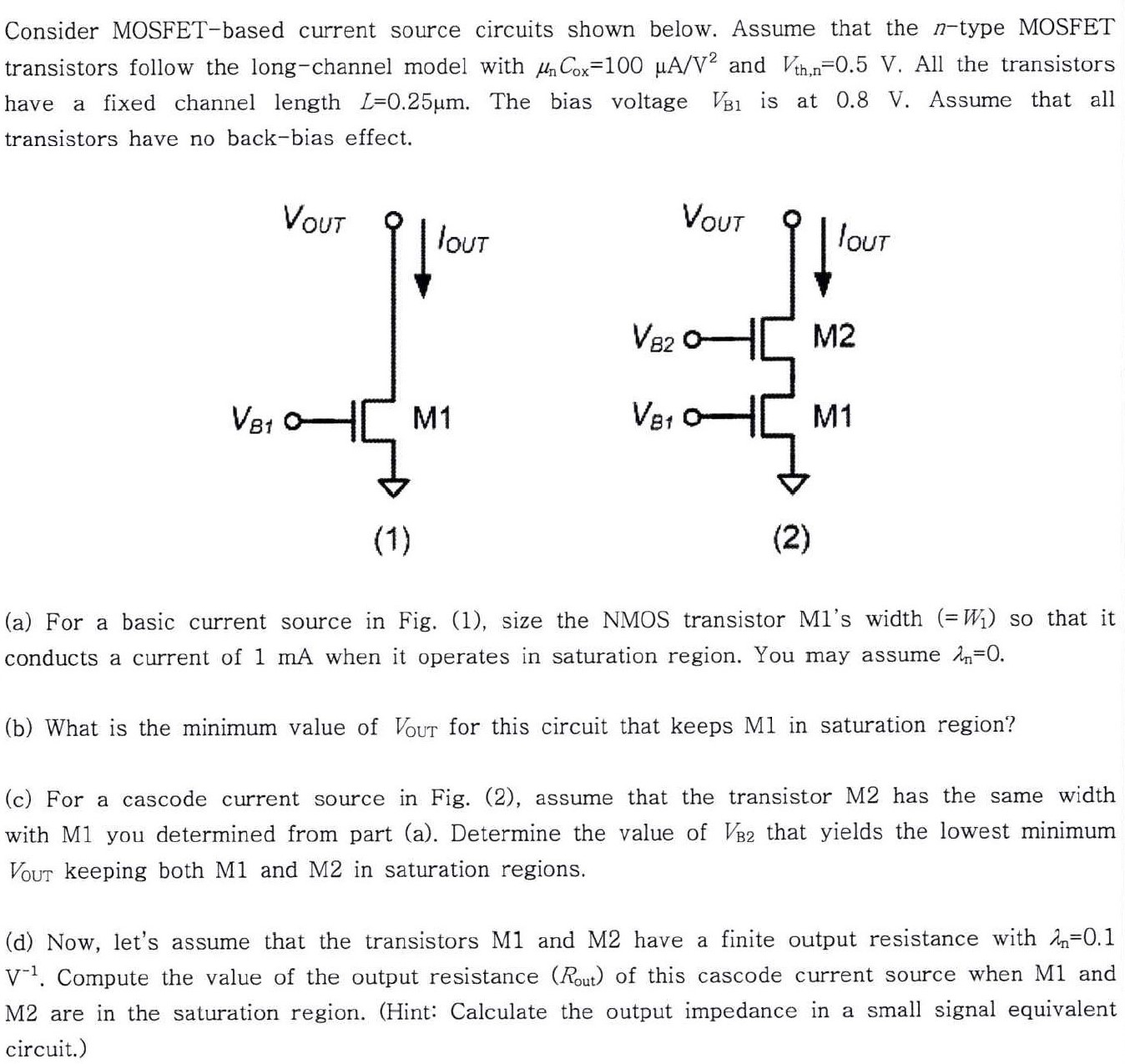
Image text
Consider the differential pair shown in Fig. 1. The power supply voltage is VDD 5 V, and all transistors have μnCox = 100 μA/V2, W/L = 2 and Vt = 1 V. You may neglect channel length modulation (VA = 1). (a) What is the value of VGS for M1 and M2 when no differential input voltage is applied and both transistors are in saturation? (b) What is maximum common mode input voltage (hint: all transistors must remain in saturation for normal operation)?