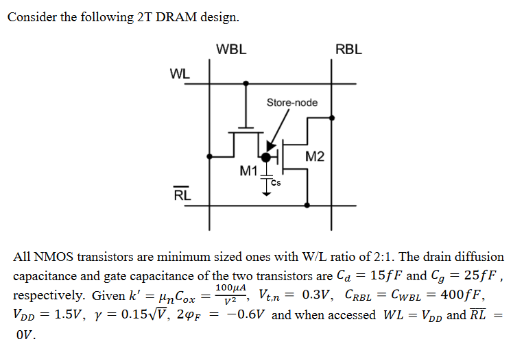
Consider the following 2 T DRAM design. All NMOS transistors are minimum sized ones with W/L ratio of 2:1. The drain diffusion capacitance and gate capacitance of the two transistors are Cd = 15 fF and Cg = 25 fF, respectively. Given k′ = μnCox = 100 μA/V2, Vt, n = 0.3 V, CRBL = CWBL = 400 fF, VDD = 1.5 V, γ = 0.15 V, 2φF = −0.6 V and when accessed WL = VDD and RL¯ = 0 V.