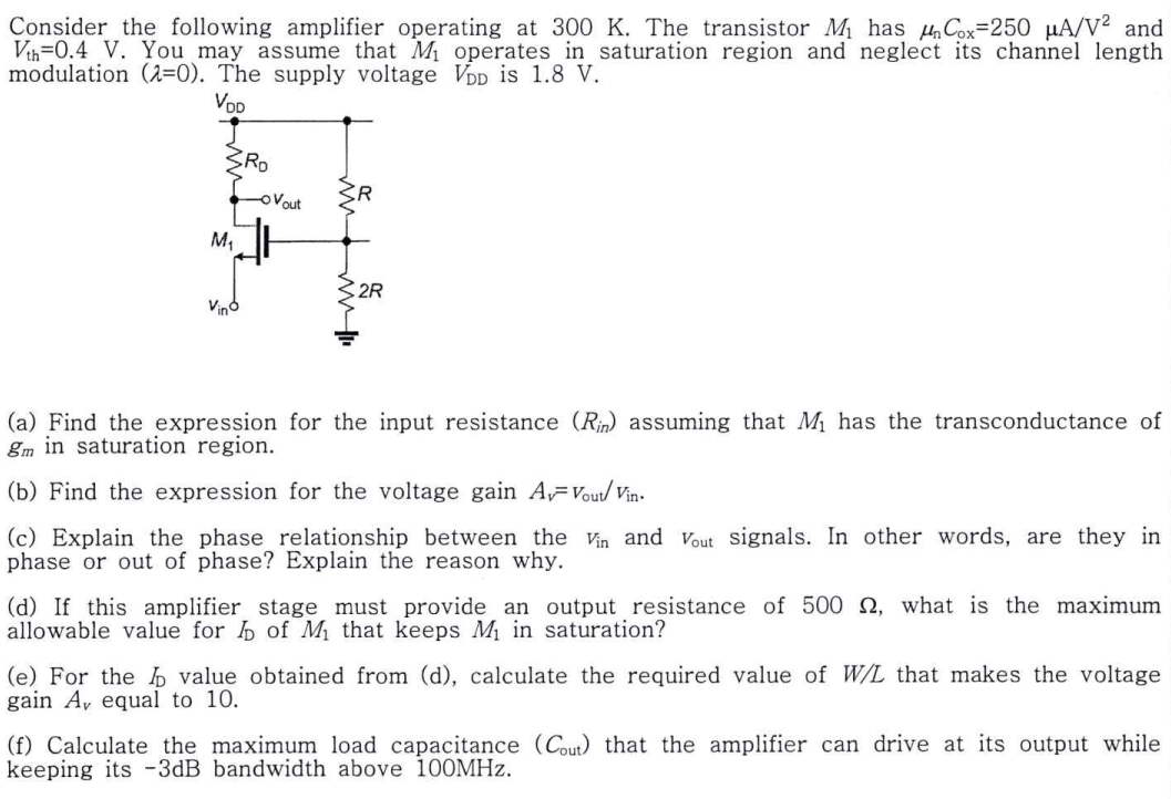
Consider the following amplifier operating at 300 K. The transistor M1 has μnCox = 250 μA/V2 and Vth = 0.4V. You may assume that M1 operates in saturation region and neglect its channel length modulation (λ = 0). The supply voltage VDD is 1.8V. (a) Find the expression for the input resistance (Rin) assuming that M1 has the transconductance of gm in saturation region. (b) Find the expression for the voltage gain AV=Vout /vin. (c) Explain the phase relationship between the vin and Vout signals. In other words, are they in phase or out of phase? Explain the reason why. (d) If this amplifier stage must provide an output resistance of 500 Ω, what is the maximum allowable value for ID of M1 that keeps M1 in saturation? (e) For the ID value obtained from (d), calculate the required value of W/L that makes the voltage gain Av equal to 10. (f) Calculate the maximum load capacitance (Cout ) that the amplifier can drive at its output while keeping its −3dB bandwidth above 100 MHz.

![(a) Figure Q2(a) shows a differential amplifier with a current source at the bottom. It is given that VDD = VSS = 15 V, ISS = 300 μA, Early effect can be ignored (λ = 0), Kn = 400 μA/V2 and VTN = 1 V. You may assume MOSFET in saturation region. (i) For single ended outputs, draw the half-circuits and derive the algebraic equations for the differential mode and common-mode gains as well as CMRR. [6 Marks] (ii) For the above case of single ended output, what should be the value of Rss to get CMRR = 100? [4 Marks] Figure Q2(a) (b) Figure Q2(b) shows a MOSFET based current mirror. Draw the AC small signal model and derive an equation for output resistance Rout as shown in the figure. You can keep your answer in terms of gm, ro etc but denote the subscript 1,2,3 etc to indicate which transistor. In other words, denote transconductance of M2 by writing gm2 and so on. [6 marks] (c) Draw the diagram of a BJT based Class B push-pull power amplifier and derive the maximum possible power efficiency of this circuit. You may ignore crossover distortion and assume |VCE(sat)| = 0 V. [9 marks]](https://www.doubtrix.com/uploads/editor/1710360410ITbaKcVzzE.jpg)