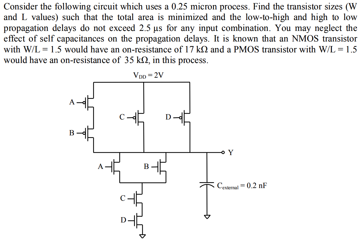
Consider the following circuit which uses a 0.25 micron process. Find the transistor sizes (W and L values) such that the total area is minimized and the low-to-high and high to low propagation delays do not exceed 2.5 µs for any input combination. You may neglect the effect of self capacitances on the propagation delays. It is known that an NMOS transistor with W/L = 1.5 would have an on-resistance of 17 kΩ and a PMOS transistor with W/L = 1.5 would have an on-resistance of 35 kΩ, in this process.
Image text
Consider the following circuit which uses a 0.25 micron process. Find the transistor sizes (W and L values) such that the total area is minimized and the low-to-high and high to low propagation delays do not exceed 2.5 µs for any input combination. You may neglect the effect of self capacitances on the propagation delays. It is known that an NMOS transistor with W/L = 1.5 would have an on-resistance of 17 kΩ and a PMOS transistor with W/L = 1.5 would have an on-resistance of 35 kΩ, in this process.