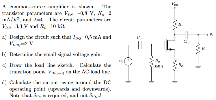
Consider the MOSFET diff-amp with the configuration in Fig. 4. The circuit parameters are V+ = 3V, V- = -3V, and IQ = 200μA. The transistor parameters are VTN = 0.4V, kn’ = 100μA/V2, W/L = 10, and λ = 0. The range of the common mode input voltage is to be -1.5 ≤ vcm ≤ +1.5V, and the common mode rejection ratio is to be CMRRdB = 50 dB. a) Design the diff-amp to produce the maximum possible differential-mode voltage gain. b) Calculate the maximum possible differential-mode voltage gain.
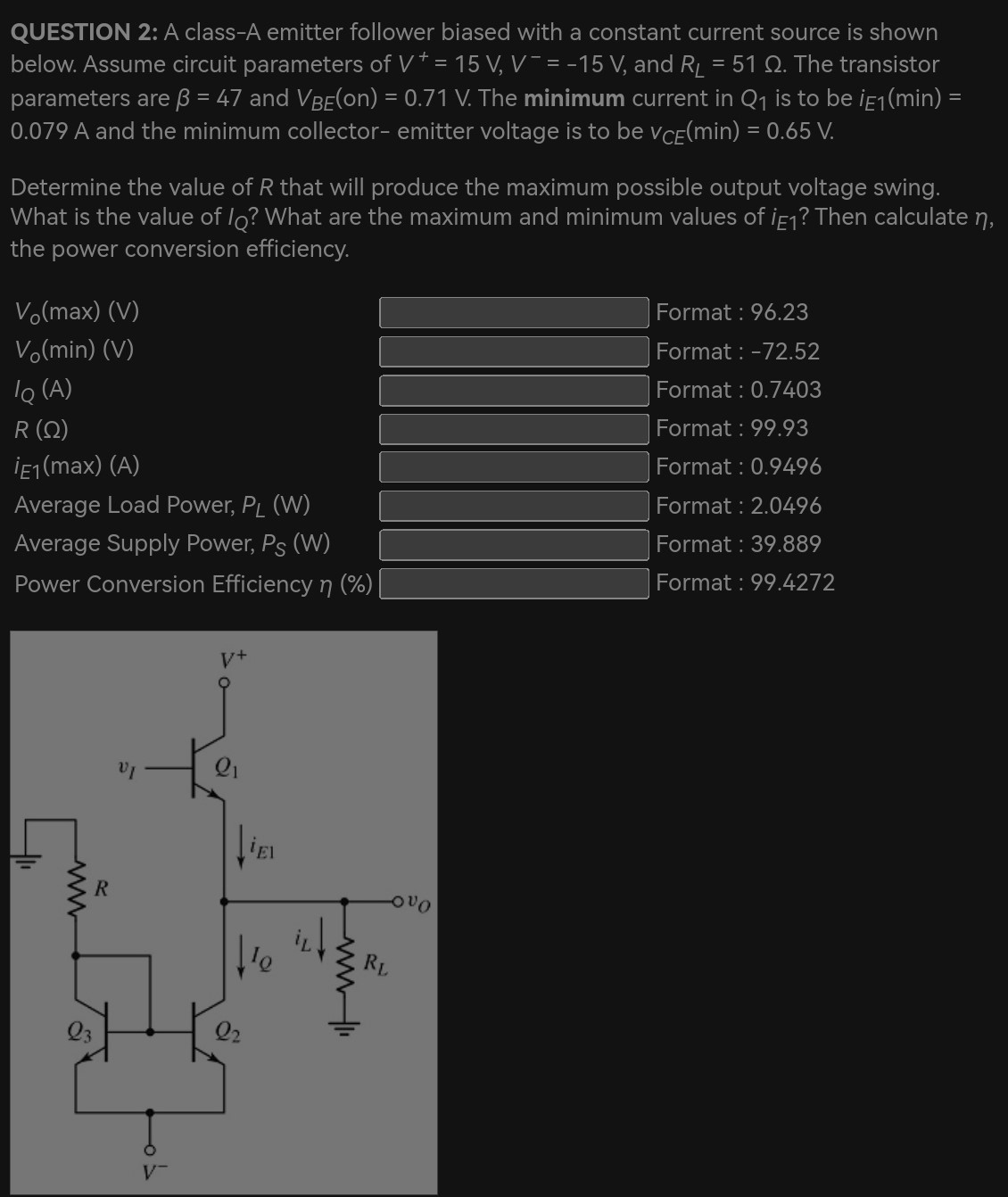
Image text
Consider the MOSFET diff-amp with the configuration in Fig. 4. The circuit parameters are V+ = 3V, V- = -3V, and IQ = 200μA. The transistor parameters are VTN = 0.4V, kn’ = 100μA/V2, W/L = 10, and λ = 0. The range of the common mode input voltage is to be -1.5 ≤ vcm ≤ +1.5V, and the common mode rejection ratio is to be CMRRdB = 50 dB. a) Design the diff-amp to produce the maximum possible differential-mode voltage gain. b) Calculate the maximum possible differential-mode voltage gain.