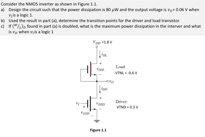
Consider the NMOS inverter as shown in Figure 1.1. a) Design the circuit such that the power dissipation is 80 μW and the output voltage is vO = 0.06 V when vI is a logic 1. b) Used the result in part (a), determine the transition points for the driver and load transistor. c) If (W/L)D found in part (a) is doubled, what is the maximum power dissipation in the inverter and what is vO when vI is a logic 1 Figure 1.1