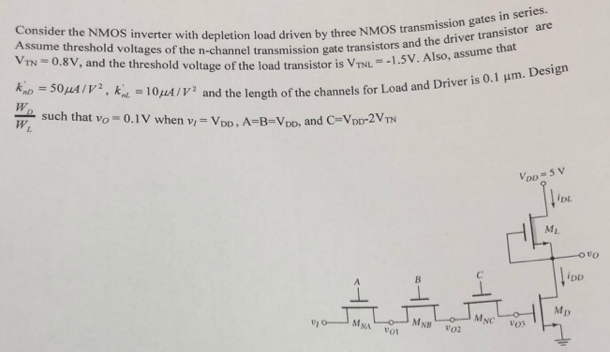
Consider the NMOS inverter with depletion load driven by three NMOS transmission gates in series. Assume threshold voltages of the n-channel transmission gate transistors and the driver transistor are VTN = 0.8 V, and the threshold voltage of the load transistor is VTNL = −1.5 V. Also, assume that kmD = 50 μA/V2, knL = 10 μA/V2 and the length of the channels for Load and Driver is 0.1 μm. Design WDWL such that vO = 0.1 V when vI = VDD, A = B = VDD, and C = VDD−2VTN
