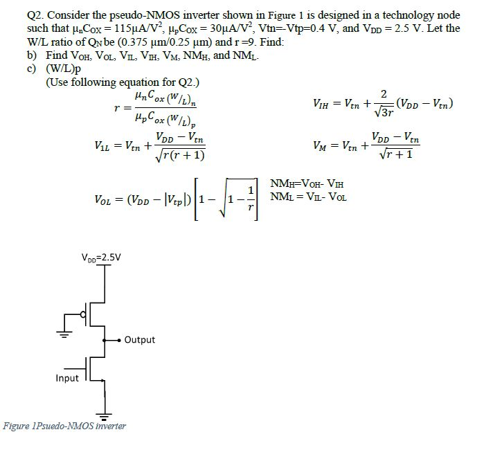
Consider the pseudo-NMOS inverter shown in Figure 1 is designed in a technology node such that unCox = 115 uA/V2, upCox = 30 uA/V2.Vtn = -Vtp = 0.4 V, and VDD = 2.5 V. Let the W/L ratio of QN be (0.375 um/0.25 um) and r =9. Find: b) Find VoH, VoL, VIL, VH, VM, NMH, and NM c) (WL)p
Image text
Consider the pseudo-NMOS inverter shown in Figure 1 is designed in a technology node such that unCox = 115 uA/V2, upCox = 30 uA/V2.Vtn = -Vtp = 0.4 V, and VDD = 2.5 V. Let the W/L ratio of QN be (0.375 um/0.25 um) and r =9. Find: b) Find VoH, VoL, VIL, VH, VM, NMH, and NM c) (WL)p